
Samsung Electronics’ SAFE™ Forum 2023: Ecosystem Development is Key to Foundry Innovation


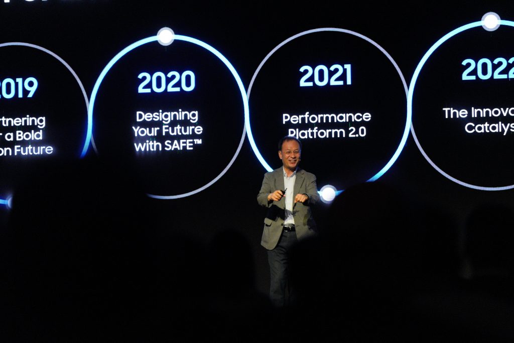
This June, Samsung Foundry’s innovations and vision for the future were unveiled in Silicon Valley, California. Following Samsung Foundry Forum 2023 on June 27 (local time), Samsung Advanced Foundry Ecosystem (SAFE™) Forum 2023 was held on June 28* with the theme of ‘Accelerate the Speed of Innovation.’
*At 0:03, we’ve corrected the date in the video from ‘June 27’ to ‘June 28.’
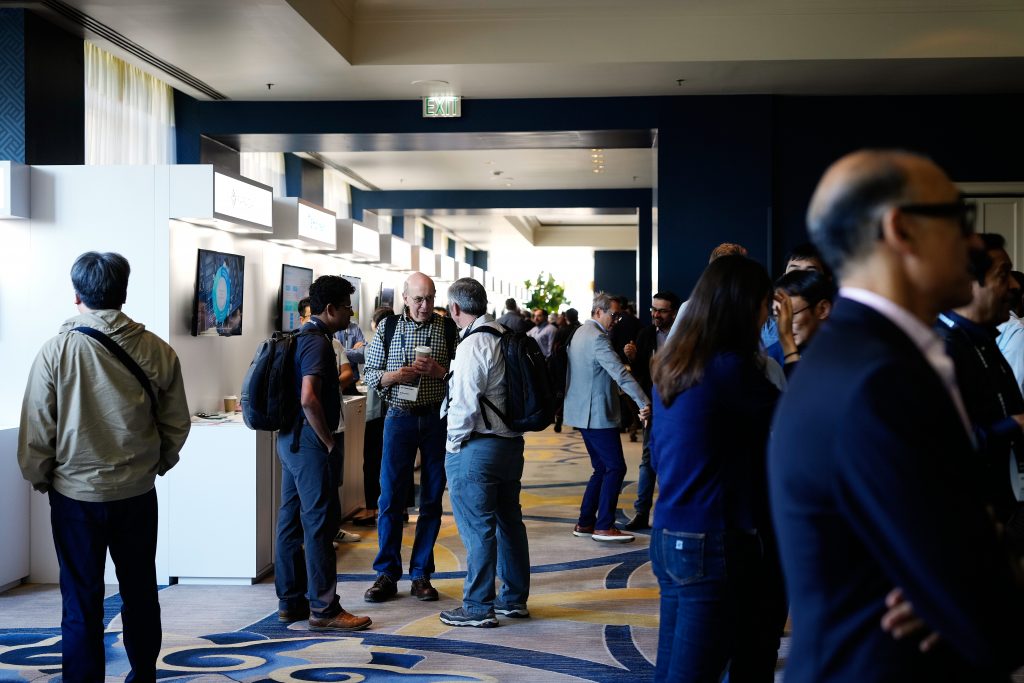
At these events, Samsung Electronics announced various advanced foundry process technologies and solutions, as well as business strategies that included plans to build new production bases. SAFE™ Forum 2023, in particular, successfully brought together technology partners working with Samsung Foundry from various fields to explore ways to foster mutual development and create a stronger semiconductor ecosystem.
Facilitating such communication in the foundry industry is crucial because developing innovative semiconductor products requires maximizing synergies by actively communicating with partners that hold diverse expertise and strengths.
Samsung Electronics is currently working with more than 100 SAFE™ partners in areas such as Intellectual Property (IP1 ), Electronic Design Automation (EDA2 ), and Outsourced Semiconductor Assembly and Test (OSAT3 ). Samsung recently announced plans to co-develop dozens of key IPs for advanced semiconductor applications with its global IP partners. These co-developed IPs will enable customers to design chips more easily, adjust for errors earlier, and reduce the time and cost of production and verification. This ensures that they can best serve the needs of global customers in a variety of markets, including AI, HPC and automotive.
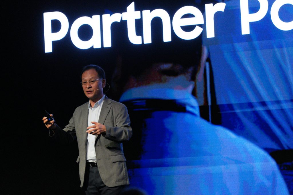
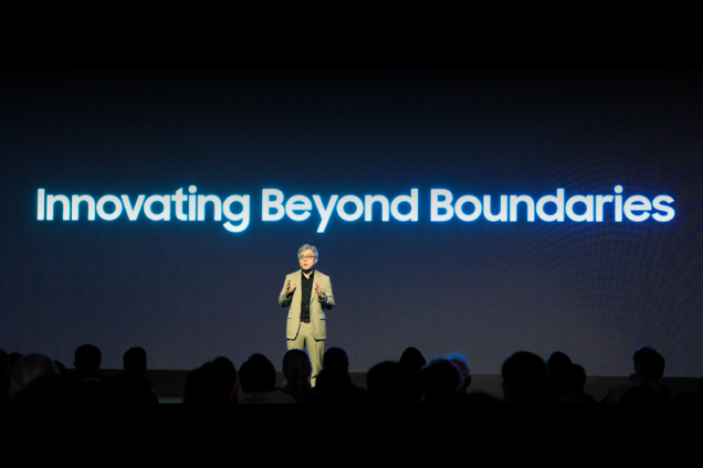
“Samsung Electronics is working with SAFE™ partners to minimize the increasing design complexity that comes with the introduction of cutting-edge processes and heterogeneous integration technology,” said Jong-wook Kye, Executive Vice President and Head of Foundry Design Platform Development at Samsung Electronics, during his keynote speech at SAFE™ Forum 2023. “It’s a much bigger ecosystem now. We are all building the ecosystem together, not only Samsung Foundry, but also everybody in this room,” he added, expressing his commitment to expanding the SAFE™ program.
1IP: Intellectual Property. A design block that implements a specific function of a semiconductor into a circuit. Designing a chip using IP can help catch design errors earlier and reduce the time and cost of production and verification.
2EDA: Electronic Design Automation. Software used to design and verify semiconductor circuits, or the industry and companies responsible for it.
3OSAT: Outsourced Semiconductor Assembly and Test. Semiconductor packaging and testing operations after the main process, or the industry and companies responsible for them.
After SAFE™ Forum 2023, the future of foundry has never looked brighter, thanks to the commitments of Samsung and its partners to build stronger foundry partnerships and to create a stronger ecosystem that works toward the common goal of customer success. Check out the video for more details, including lively interviews with key partners!
Related tag
#global partners
#SAFE
#SAFE 2023
#SAFE Collaborate
#SAFE Forum 2023 Highlights
#SAFE Samsung Foundry
#Samsung
#Samsung Advanced Foundry Ecosystem
#Samsung Electronics
#samsung semiconductor newsroomSAFE
#semiconductor
Related Stories
-
 2023.06.30D-VTG Technology of ISOCELL Image Sensor, Samsung’s new pixel technology takes ultra-high resolution to the next level.
 -
 2023.06.28Why Foundry is Crucial: Solutions to the AI Era Unveiled at Samsung Foundry Forum 2023
 -
 2023.06.14Samsung Electronics Powers Enhanced Customer Development Support with Expanded SAFE Program