D-VTG Technology of ISOCELL Image Sensor, Samsung’s new pixel technology takes ultra-high resolution to the next level.


In January, Samsung unveiled ISOCELL HP2, a 200-megapixel (MP) image sensor, for ultra-high resolution photos with epic details for future premium smartphones and unpacked Galaxy S23 Ultra with ISOCELL HP2 at the Galaxy Unpacked event in February 2023. For premium smartphone users including both professionals and consumers who want to take their photography to the next level, Galaxy S23 Ultra with ISOCELL HP2 has opened new possibilities with more pixels and epic details.
To provide the best possible pixel performance and detailed, seamless photos in all lighting conditions, Samsung combines a range of fresh, advanced technologies and improved the pixel structure to increase light absorption. The Dual Vertical Transfer Gate (D-VTG), a redesigned pixel structure, is a key component of the ISOCELL HP2’s ability to improve the appearance of color and detail in each pixel, even in bright conditions.
Let’s take a closer look at this technology, which is key to the performance of ISOCELL’s current and future image sensors.
Understanding pixel structures and transfer gate
Light passes through a microlens and a color filter in a pixel array. A photodiode converts the light into negatively charged electrons. These electrons are stored in a floating diffusion via a transfer gate. The electrons are then passed through a circuit where an analog-to-digital converter (ADC) generates a voltage proportional to the amount of charge and converts it into a digital signal.
A transfer gate, similar to a switch, can control the movement of electrons from a photodiode to a floating diffusion. In particular, the maximum number of electrons that a transfer gate can pass has a significant effect on the performance of the image sensor. If the transfer gate can pass more electrons, the size of the photodiode within the pixel can be increased. As a result, the maximum transfer capacity of the transfer gate affects several image quality performance metrics, such as dynamic range.
As image sensors become smaller and more pixel denser, the size of the transfer gate in contact with the photodiode must shrink. However, the smaller the transfer gate, the fewer electrons that can be transferred and the more noise problems that arise. In particular, Samsung’s ISOCELL pixel technology has reduced inter-pixel interference by creating a physical barrier, front deep trench isolation (FDTI), between pixels. Creating a wall between pixels reduces the space for photodiodes and therefore, the amount of light that can be captured.
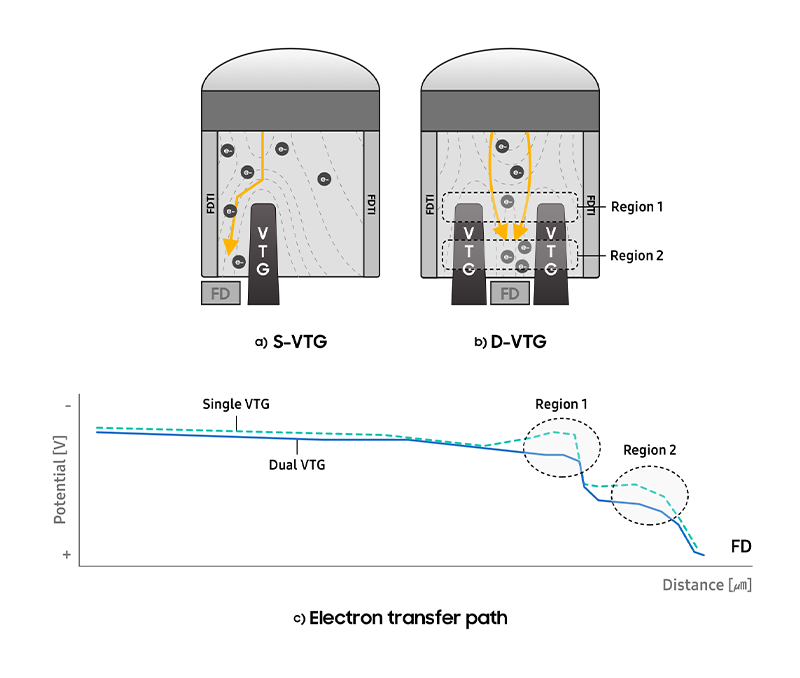
To overcome this drawback, Vertical Transfer Gate (VTG) technology is used, which changes the structure of the transfer gate vertically. Transfer gate is located below the photodiode, and by changing the structure of transfer gate from horizontal to vertical, the photodiode can be formed deeper within the pixel, allowing enough electrons to be captured in a smaller area. Transfer gate allows more electrons to be transferred to the floating diffusion and more light information to be captured.
Development of Dual VTG
The demand for ultra-high resolution in mobile image sensors has increased, and Samsung has moved beyond 108 megapixels to 200 megapixels. Due to the structure of the optical module and the limitations of the image sensor format in smartphones, this requires a smaller pixel size, and the smaller the pixel pitch, the smaller the photodiode area. To address this, Samsung has continuously improved its ISOCELL pixel technology based on FDTI structure to 0.64㎛ pixels and maintained Full Well Capacity (FWC) at approximately 6,000e- level through DTI size reduction and optimized Plasma-assisted doping (PLAD).
To improve performance of ultra-high resolution image sensors with even smaller sized pixels, Samsung developed D-VTG (Dual Vertical Transfer Gate) technology which integrates two VTGs in one pixel, and introduced it in ISOCELL HP2 image sensor. By implementing two VTGs, Samsung not only increased the controllability of individual transfer gate voltages to improve transfer capability compared to a single VTG, but also optimized the gap between VTGs, depth and taper slope to maximize electron transfer.
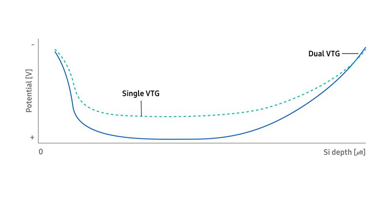
As shown in Figure 1, the number of electrons travelling along the VTGs, i.e., the potential value, shows that the D-VTG has a higher potential value than the S-VTG (Single VTG) in both regions 1 and 2.
Simulations were also carried out where the distance between two VTGs was reduced from 130 nm to 20 nm and the size of the VTGs was also reduced, as shown in the diagram below. In region 1, the potential value increased as the VTG size increased, whereas in region 2, the potential value increased as the gap between the VTGs decreased.
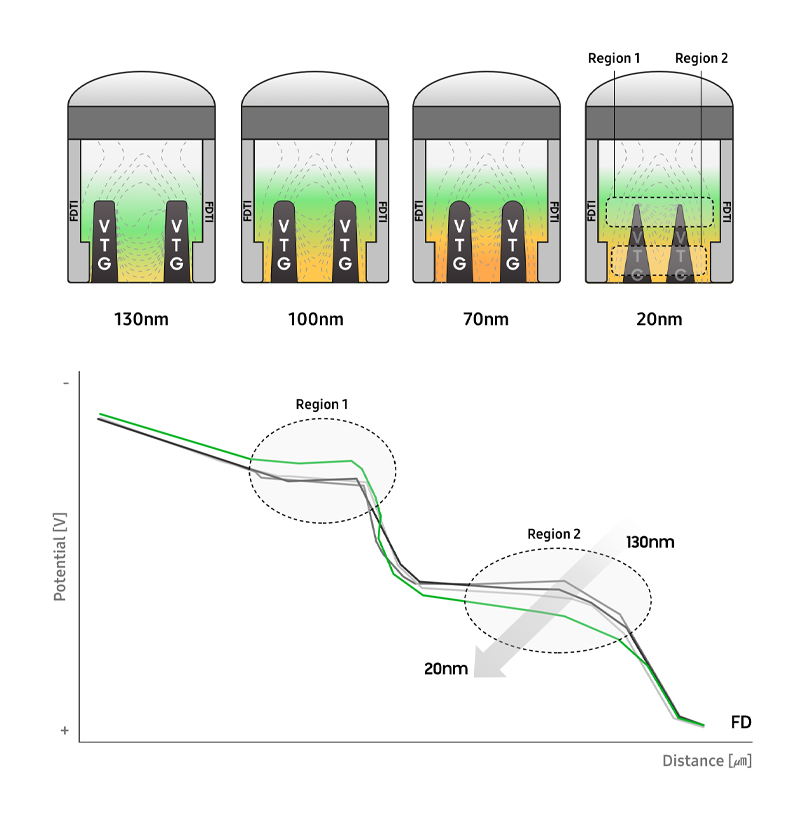
Figure 2. Potential profile and electron transfer path in region 1 and in region 2 according to D-VTG gap
Performance improvement
Figure 3 shows the image delay results for S-VTG and D-VTG measured at the same FWC. Image delay means that electrons that have not passed through the transfer gate in this frame move and pass through in the next frame, affecting color reproduction. At 1.5V, the D-VTG had no image delay, but the S-VTG had an image delay of about 13 LSB.
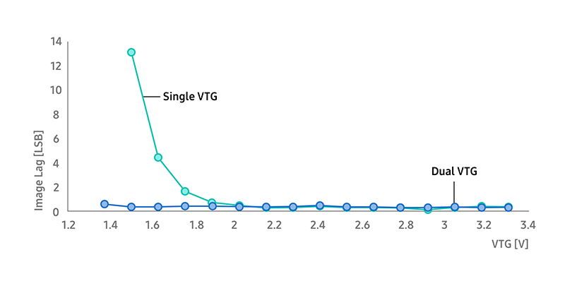
This means that for the same voltage, D-VTG has a higher transfer efficiency than S-VTG, allowing the photodiode in the pixel to be formed deeper to accept more light, as shown in Figure 4.
As a result, the D-VTG has up to approximately 66% higher FWC compared to the S-VTG, while noise levels such as random noise (RN) and random telegraph signal (RTS) and white spot (defective pixels with leakage current due to defects) characteristics remain similar.
In case of ISOCELL HP2, each pixel absorbs 33% more electrons than the predecessor 200MP image sensor. By being able to use more electrons per pixel, color reproduction in bright light conditions is remarkably enhanced. ISOCELL HP2 is Samsung’s first image sensor that adopted the D-VTG technology that enables sufficient FWC even with small pixel sizes. Samsung plans to apply this innovative technology to various image sensor lineups to provide consumers with a better camera experience.
Source: J. Yun et al., “A 0.6 ㎛ Small Pixel for High Resolution CMOS Image Sensor with Full Well Capacity of 10,000e- by Dual Vertical Transfer Gate Technology,” 2022 IEEE Symposium on VLSI Technology and Circuits (VLSI Technology and Circuits), Honolulu, HI, USA, 2022, pp. 351-352, doi: 10.1109/VLSITechnologyandCir46769.2022.9830254. (Link)

Related tag
#D-VTG
#D-VTG Technology
#ISOCELL
#ISOCELL HP2
#ISOCELL Image Sensor
#Samsung
#Samsung Image Sensor
#samsung semiconductor newsroom
#Samsung’s new pixel technology
#semiconductor