Featured Stories
69 posts
-
Technology 2026.07.08
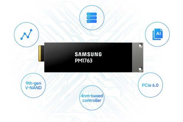
[Infographic] Samsung PM1763 SSD: A Core Storage Solution for Next-Generation AI Platforms
When Solid State Drives (SSDs) first gained widespread adoption in the 2000s, they quickly replaced Hard Disk Drives (HDDs) as the standard storage solution...
-
Technology 2026.07.03
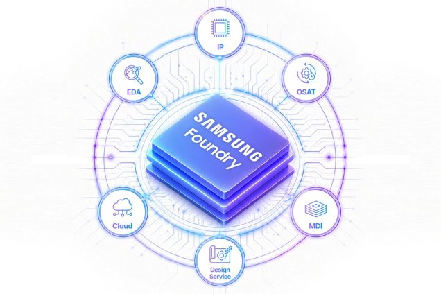
[Infographic] Teamwork Behind Cutting-Edge Chip Manufacturing: How Samsung Foundry’s SAFE™ Ecosystem Powers Next-Generation Semiconductor Innovation
Enabling Faster, More Reliable and Higher-Performance Chip Production An advanced System on Chip (SoC)—a semiconductor that serves as the brain behind AI...
-
Technology 2026.06.23
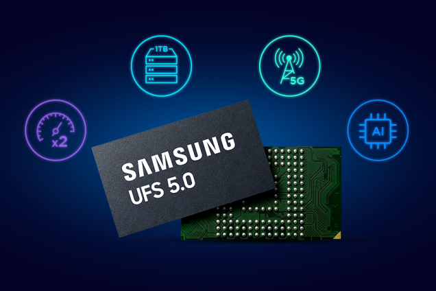
[Infographic] UFS 5.0 Memory: The Optimal Solution for On-Device AI
Samsung Electronics has announced the development of its next-generation Universal Flash Storage (UFS) 5.0 mobile memory solution, setting a new benchmark...
-
Technology 2026.06.17
Breaking Through the Limits of Horizontal Scaling with Vertical Innovation
Samsung Semiconductor R&D Center Demonstrates Industry’s First42nm Gate-Pitch 3D-Stacked Transistor Selected as the Best Paper from over 1,000...

-
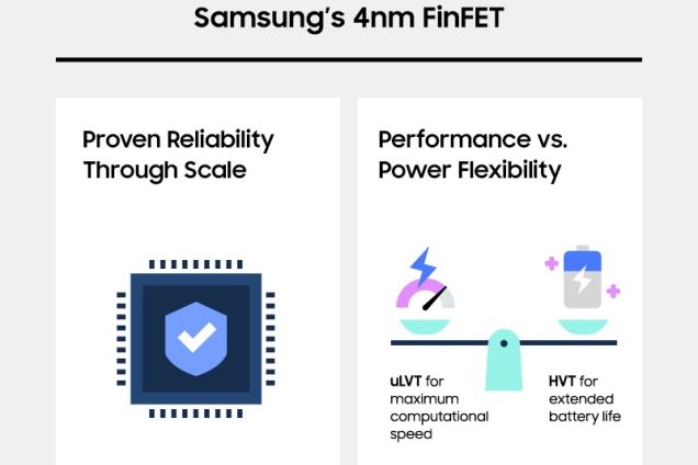
Technology 2026.04.30
Samsung Foundry 4nm FinFET: The Best of Both Worlds for Performance and Reliability
One of the hardest decisions in semiconductor design is choosing between cutting-edge and proven process nodes. Leading-edge processes deliver top-tier...
-
Technology 2026.03.17
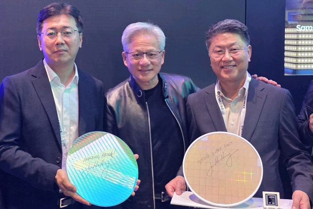
[Video] Architecting the AI Era: Samsung Electronics and NVIDIA Define the Future at GTC 2026
Samsung Electronics, a global leader in advanced semiconductor technology, took center stage at NVIDIA GTC 2026 to showcase its vision for the future of...