
Samsung Electronics Powers Enhanced Customer Development Support with Expanded SAFE Program


SEOUL, Korea – June 12, 2023 – Samsung Electronics Co., Ltd., a world leader in advanced semiconductor technology, today announced an expansion of its foundry ecosystem to offer a broader Intellectual Property (IP) portfolio for next-generation semiconductor design and production. Samsung’s foundry business has secured the support of leading IP providers to offer a wide range of IPs covering important market segments such as AI, GPU, HPC, automotive and mobile applications. The company expects greater access to a wide range of proven IP to enable faster and more effective System on Chip (SoC) implementation for customers.
The expanded IP ecosystem includes dozens of new IPs that are optimized for Samsung Foundry’s 3 to 8-nanometer processes.
“Samsung is actively pursuing the expansion of our cutting-edge IP portfolio, prioritizing the success of our customers above all,” said Jongshin Shin, corporate executive vice president of Foundry IP Development at Samsung Electronics. “We are pleased to announce a significant expansion of the SAFE program to further expand our IP portfolio to effectively meet the needs of our customers in product innovation and production.”
Samsung provides the IP ecosystem with the latest foundry process information needed to develop progressive IP such as Process Design Kits (PDK) and Design Methodologies (DM). IP providers then develop IP optimized for Samsung foundry processes to provide to global fabless customers. After that, the SAFE program provides customers with certified design flows and access to advanced packaging solutions, which further enables fast time-to-market.
Fabless customers will be able to utilize IP optimized for Samsung’s foundry processes, aligned with the product development stage. Customers will be able to reduce errors from the earliest stages of design as well as reduce the time and cost of prototyping, validation and mass production.
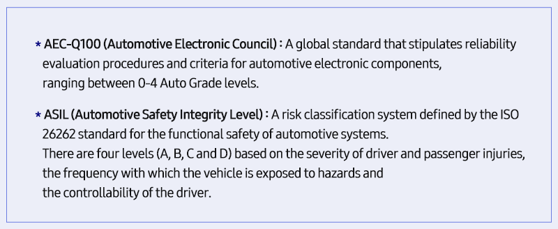
Samsung will collaborate with the IP ecosystem to develop high-speed interface IP for next-generation protocols such as PCIe 6.0, 112G SerDes and DDR5/LPDDR5X/GDDR7. The company is also seeking to strengthen its portfolio to develop IP for Compute Express Link (CXL) 3.0 and Universal Chiplet Interface express (UCIe), which are used on leading-edge packages such as chiplets. Additionally, it will support automotive IP solutions that meet the highest levels of automotive semiconductor reliability standards and quality standards, such as the AEC-Q100* and ASIL levels*.
Further details of the IP ecosystem as well as Samsung’s roadmap and strategy for IP development will be unveiled at the SAFE Forum on June 28 in San Jose, California.
Quotes from IP Partners:
[Synopsys]
John Koeter, senior vice president of product management and strategy for IP at Synopsys
“Our extensive co-optimization efforts with Samsung across both EDA and IP help automotive, mobile, HPC, and multi-die system architects cope with the inherent challenges of designing chips for advanced process technologies. This extension of our decades-long collaboration provides designers with a low-risk path to achieving their design requirements and quickly launching differentiated products to the market.”
Synopsys is collaborating with Samsung to enhance the Synopsys IP offering for Samsung’s advanced 8LPU, SF5, SF4 and SF3 processes. The collaboration includes Foundation IP (logic libraries, embedded memories, TCAMs, and GPIOs), eUSB2, USB 2.0/3.0/3.1/4.0, USB-C/DisplayPort, PCI Express 3.0/4.0/5.0/6.0, 112G Ethernet, Multi-Protocol 16G/32G PHYs, UCIe, HDMI 2.1, LPDDR5X/5/4X/4, DDR5/4/3, SD3.0/eMMC 5.1, MIPI C/D PHY, and MIPI M-PHY G4/G5. In addition, Synopsys will optimize IP for Samsung’s SF5A and SF4A automotive process nodes to meet stringent Grade 1 or Grade 2 temperature and AEC-Q100 reliability requirements, enabling automotive chip designers to reduce their design effort and accelerate AEC-Q100 qualification.
[Cadence]
Rishi Chugh, vice president of product marketing in the IP Group at Cadence:
“Continuing our deep and broad collaboration with Samsung, Cadence is committed to expanding our IP portfolio offering to address our customers’ evolving design requirements. Through this partnership, we will accelerate market adoption of Samsung’s 8LPU, SF5, SF4 and SF3 process nodes by enabling a rich set of high-performance interface IP including PCIe, 112G-ULR, DDR5, UCIe, USB and GDDR. This advanced technology portfolio offering from Cadence addresses the demanding PPA requirements for HPC, AI/ML, networking, storage, and automotive applications as well as enables chiplet-based designs to enter the mainstream.”
[Alphawave]
Tony Pialis, CEO, and co-founder of Alphawave Semi

“Data center connectivity is undergoing a remarkable transformation due to the rise of generative AI, ushering in an era of high performance chiplet-enabled silicon. Besides enabling the AI infrastructure, Alphawave Semi technology also enables connectivity in the datacenters that house AI solutions. Alphawave Semi is pleased to expand our deep collaboration with Samsung Foundry to the 3nm node, leveraging our most advanced high-speed connectivity IP technologies that provide new levels of performance, flexibility, and scalability to hyperscalars and data-infrastructure customers.”
Alphawave Semi and Samsung have been collaborating over multiple customer designs and process generations, including 5nm and 4nm, and now 3nm. Alphawave Semi’s high-performance connectivity PHY IP including 112 Gbps Ethernet and PCIe Gen6/CXL3.0, and Universal Chiplet ExpressTM (UCIeTM) are available in the Samsung Foundry nodes. Alphawave Semi also offers them as fully integrated IP subsystems together with controller IP. For more information, please contact Alphawave Semi at info@awavesemi.com.
Related tag
#AEC-Q100
#ASIL levels
#Foundry
#IP portfolio
#SAFE Program
#Samsung
#Samsung Electronics
#Samsung Foundry
#Samsung Semiconductor
#samsung semiconductor newsroom
#Samsung will collaborate with the IP ecosystem
Related Stories
-
 2023.06.28Why Foundry is Crucial: Solutions to the AI Era Unveiled at Samsung Foundry Forum 2023
 -
 2023.06.13[Want a Byte? Ep.4] How Samsung’s Mobile GPU Brings More Immersive Gaming to Smartphones with Hyper-realistic Graphics: Xclipse
 -
 2023.06.02Samsung’s Biometric Card IC: All-in-one fingerprint solution for a new payment experience.