Samsung V-NAND : A Landmark of the Hyperscale AI Era


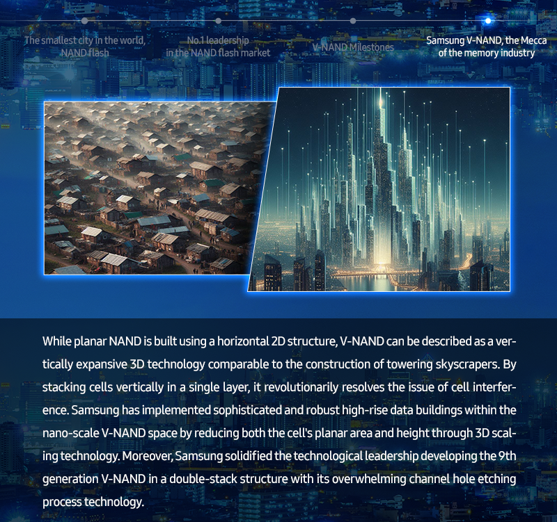
Samsung solidified its leadership in the NAND flash market by commencing production of the industry’s first “1Tb (terabit) TLC (Triple Level Cell)* 9th generation V-NAND” in April. It boasts approximately 1.5 times higher bit density* than the previous generation, thanks to the implementation of industry’s smallest cell size and thinnest mold*. It features technologies such as cell interference avoidance and cell life extension to control interference phenomena* and enhance product speed, power efficiency, quality, and reliability.
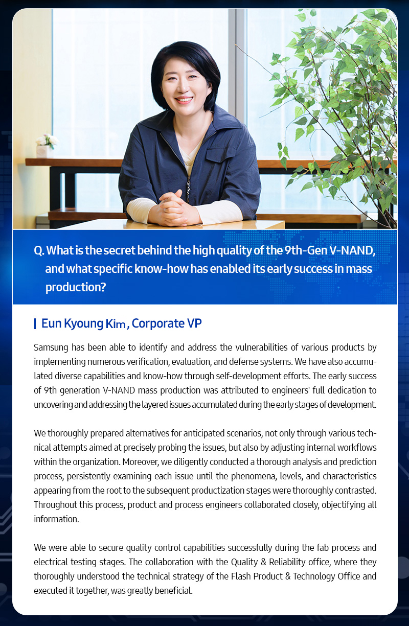
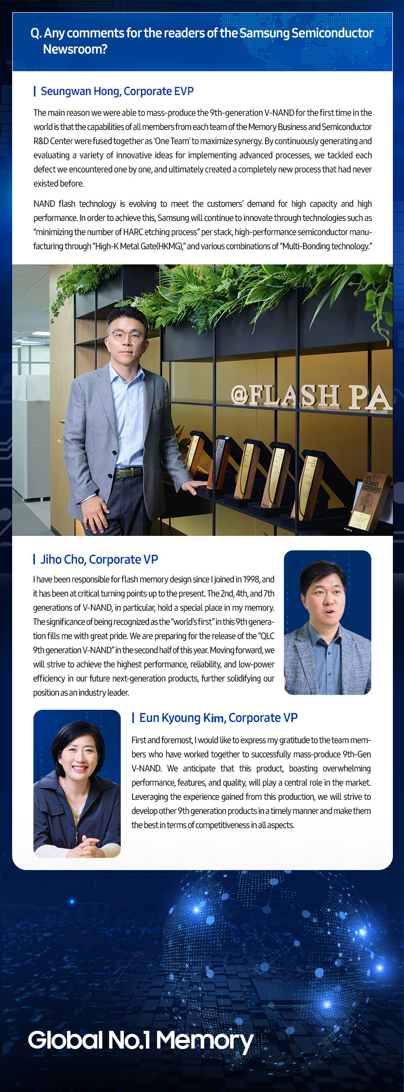
Today, the newsroom had the opportunity to meet with Jay Hyun, the Corporate VP of Product Planning, Seungwan Hong (Corporate EVP), Eun Kyoung Kim (Corporate VP), and Jiho Cho (Corporate VP) of Flash Product & Technology. These individuals are responsible for the planning and development of the revolutionary 9th generation V-NAND. Join us as we venture into the world of Samsung V-NAND and discover the exciting possibilities it brings in the era of AI.
* TLC (Triple Level Cell): a structure that can store 3 bits of data in a single cell.
* Bit Density: the number of bits stored per unit area.
* Mold: the layer of word lines (wiring responsible for controlling the on/off state of transistors) that drives the cell.
* Interference Phenomena: a phenomenon where electrons leak or adjacent cells are affected due to narrow spacing between cells.


Since becoming the world’s number one in NAND flash memory in 2002, Samsung has been leading the market and introducing groundbreaking technologies. Following the successful 9th-Gen V-NAND mass production, which can be considered the fruit of a long journey, Samsung plans to continue shaping a sophisticated future through relentless innovation and the development of cutting-edge memory technologies.
Related tag
#interview #High-K Metal Gate #V-NAND #HARC #QLC #TCMC #TLC #3D V-nand #9th Gen V-NAND #CTF Structure #Dummy channel holes #multi-bonding #Channel hole etch #Contact etch #Floating gate