
[Editorial] How Samsung Is Breaking New Ground in DRAM for the AI Era


In late 2022, ChatGPT sent shockwaves around the world. In a mere five days, the service had attracted one million subscribers. In two months, this number had surged to 100 million setting the record for fastest sign-up rate that any application has ever seen. ChatGPT has captivated so many users because it offers a broad and versatile range of features with a never-before-seen conversational fluency often indistinguishable from text-based discussions with humans. In short, it has marked a new era of hyperscale AI.
ChatGPT is a large language model (LLM) that uses a vast dataset encompassing 175 billion parameters as its basis for training. As a result, the key to effective delivery of its services lies in high-performance semiconductors. In order to smoothly process such a large volume of data, memory semiconductors need to provide optimized capabilities spanning high performance, high bandwidth and minimized latency for faster reading and writing.
In this new age of hyperscale AI, technological advancements in memory semiconductors and the enhancement of their performance is crucial. Samsung Electronics is deploying its unique technologies to develop a variety of memory solutions through 40 years of industry-leading expertise to expand its AI semiconductor ecosystem.
.
High-performance HBM: A Vital Component of the AI Era
In 2016, Samsung commercialized the industry’s first high-bandwidth memory (HBM) for high-performance computing (HPC) and pursued opportunities to expand the AI memory market.
A year later, in 2017, Samsung introduced its 8-layer stacked HBM2. When compared to GDDR5 – the fastest memory available at the time – HBM2 delivered eight times the speed. Through HBM2, Samsung successfully demonstrated the viability of 3D stacking technology, which would go on to be an essential component of the new HPC/AI landscape.
Later on, Samsung mass-produced HBM2E and HBM3, and has developed 9.8 gigabits-per-second (Gbps) HBM3E, which we’ll soon start sampling to customers in our drive to enrich the HPC/AI ecosystem.
Looking ahead, HBM4 is expected to be introduced by 2025 with technologies optimized for high thermal properties in development, such as non-conductive film (NCF)[1] assembly and hybrid copper bonding (HCB)[2].
Samsung launched its AVP (AdVanced Package) Business Team in early 2023 to strengthen advanced packaging technology and maximize synergy across business units. Alongside HBM, Samsung will provide advanced custom turnkey packaging services — including 2.5D[3] and 3D[4] advanced packaging solutions — ideal for the age of HPC and AI.

.
DDR5 DRAM: Record-setting Capacity and Performance
High-end central processing units (CPUs) for AI services require more than 100 cores, with each needing to be accompanied by sufficient memory. To successfully push the physically limited capacity of packages further, process technologies must reduce the size of a single DRAM[5] chip to the extent possible. Equally important is design technology that ensures components are placed efficiently within the form factor and performance that matches specifications.
The new 32-gigabit (Gb) DDR5 DRAM possesses a capacity 500,000 times larger than the 64-kilobit (Kb) DRAM developed 40 years ago. Architectural enhancements have effectively doubled the capacity of 16Gb DRAM, all within the same package size, allowing the fabrication of 128-gigabyte (GB) modules without using Through Silicon Via (TSV). This allows for more cost-effective production, heightened productivity and a 10% power consumption improvement.
The new DDR5 DRAM will enable the implementation of modules of up to one terabyte (TB). Relevant applications will be data centers that require high capacity, as well as future memory solutions like MRDIMM and CXL Memory Module.
Meanwhile, Samsung’s DDR5 12 nanometer (nm)-class DRAM — the industry’s most advanced — boosts productivity by approximately 20% compared to the previous generation. This differentiated technology allows for outstanding performance and power efficiency while supporting a maximum operating speed of 7.2Gbps. With an operating speed like this, two 30GB UHD movies can be processed within a mere second. DDR5 12-nm-class DRAM will meet diverse customer needs by catering to numerous applications, from data centers to the realm of HPC and AI.
.
PIM: A New Paradigm in the Memory Market
The memory bottleneck stemming from the von Neumann architecture is a key hurdle for large data applications like ChatGPT.
To overcome this, Samsung developed the industry’s first HBM-PIM (Processing-In-Memory) solution in 2018. HBM-PIM enabled in-memory computation at excellent energy efficiency levels. Also, this breakthrough led to the standardization of PIM platforms while establishing a new industry/academic ecosystem. HBM-PIM addressed the bottleneck in memory bandwidth by embedding data computation functions within DRAM, leading up to 12-fold performance improvements. Specific functions, such as voice recognition, became four times more power-efficient.
Related research to enhance system performance is also ongoing. Alongside generative AI scalability, we are studying how to configure PIM architectures on DRAM using CXL interfaces.
.
Building New Markets for Tomorrow’s Form Factors
Until now, DRAM used in laptops and PCs were typically either LPDDR or So-DIMM[6]. So-DIMMs can be detachable but have limitations with transmission speed and space efficiency. LPDDR, by contrast, is compact and power efficient, but soldered onto the motherboard. To bridge this gap, Samsung developed the industry’s first Low Power Compression Attached Memory Module (LPCAMM), a module product based on LPDDR DRAM, combines the best traits of both.
Samsung’s groundbreaking LPCAMM is pioneering a new LPDDR form factor market. It enables high-performance and low-power usage but is also removable, offering the flexibility for repairs or upgrades. The mounting area, meanwhile, is up to 60% than that of So-DIMMs, freeing up internal space while improving performance and power efficiency by up to 50% and 70%, respectively.
As performance and power efficiency of memory products are both important, LPCAMM has the potential to be used for a variety of applications beyond laptops and PCs, such as data centers.
.
Innovating for a Future Powered by Semiconductors
For more than 40 years, Samsung Electronics has made technological breakthroughs through a steadfast commitment to innovation. Through our distinctive competitiveness approach, we will continue to release products above and beyond today’s expectations while pre-empting the needs of tomorrow’s technologies. We will provide ultra-high performance, ultra-high capacity and ultra-low power memory solutions required in the new AI era, with a particular focus on the major DRAM market inflection point of the sub-10-nm process.
As we’ve always been, Samsung will remain at the epicenter of technological innovation, developing semiconductors to meet the needs of our rapidly changing world.
.
[1]NCF (non-conductive film): A polymer layer that protects solder joints from insulation and mechanical shock between stacked chips.
[2]HCB (hybrid copper bonding): A next-generation bonding technology that uses copper (conductor) and oxide film (insulator) instead of conventional solder.
[3]2.5D package: A package which integrates a single-layer logic semiconductor and a multi-layer memory semiconductor together on a substrate.
[4]3D package: A package in which multiple logic/memory semiconductors are vertically integrated.
[5]DRAM: Dynamic Random Access Memory
[6]So-DIMM : Small outline Dual In-line Memory Module
.
Related tag
Related Stories
-
 2023.10.12Samsung Austin Semiconductor Pumps $13.6 Billion into Central Texas Economy in 2022
 -
 2023.10.06Samsung Partners with Leading Engineering Schools Across the U.S. to Bolster the Semiconductor Ecosystem with $5.7 Million in Donations
 -
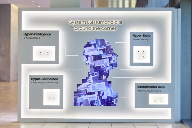 2023.10.06The System LSI Humanoid Is Here! Advanced Technology for the Hyper-Connected Era Unveiled at Samsung System LSI Tech Day 2023