[Infographic] Teamwork Behind Cutting-Edge Chip Manufacturing: How Samsung Foundry’s SAFE™ Ecosystem Powers Next-Generation Semiconductor Innovation


Enabling Faster, More Reliable and Higher-Performance Chip Production
An advanced System on Chip (SoC)—a semiconductor that serves as the brain behind AI applications, smartphones and automobiles—cannot be built by a single company alone. Developing a modern SoC requires close collaboration among a wide range of specialized companies, including fabless firms that design chips without manufacturing facilities, electronic design automation (EDA) providers that develop chip design software, partners supplying intellectual property (IP) and foundries that manufacture the chips. Such collaboration is essential to successfully bring a sing SoC from idea to production.
Through the Samsung Advanced Foundry Ecosystem (SAFE™), Samsung Foundry serves as a central hub that connects customers and ecosystem partners.
What Is SAFE™? – Connecting Every Stage of Chip Development
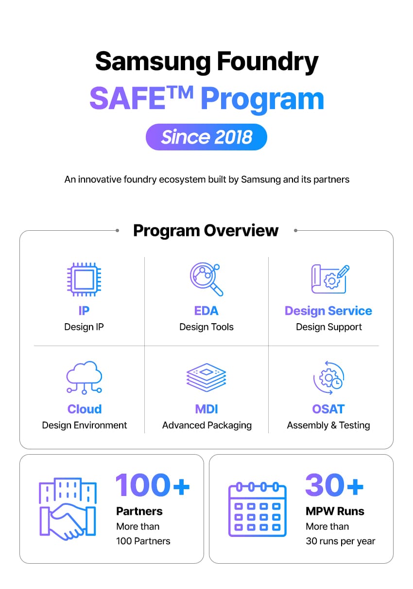
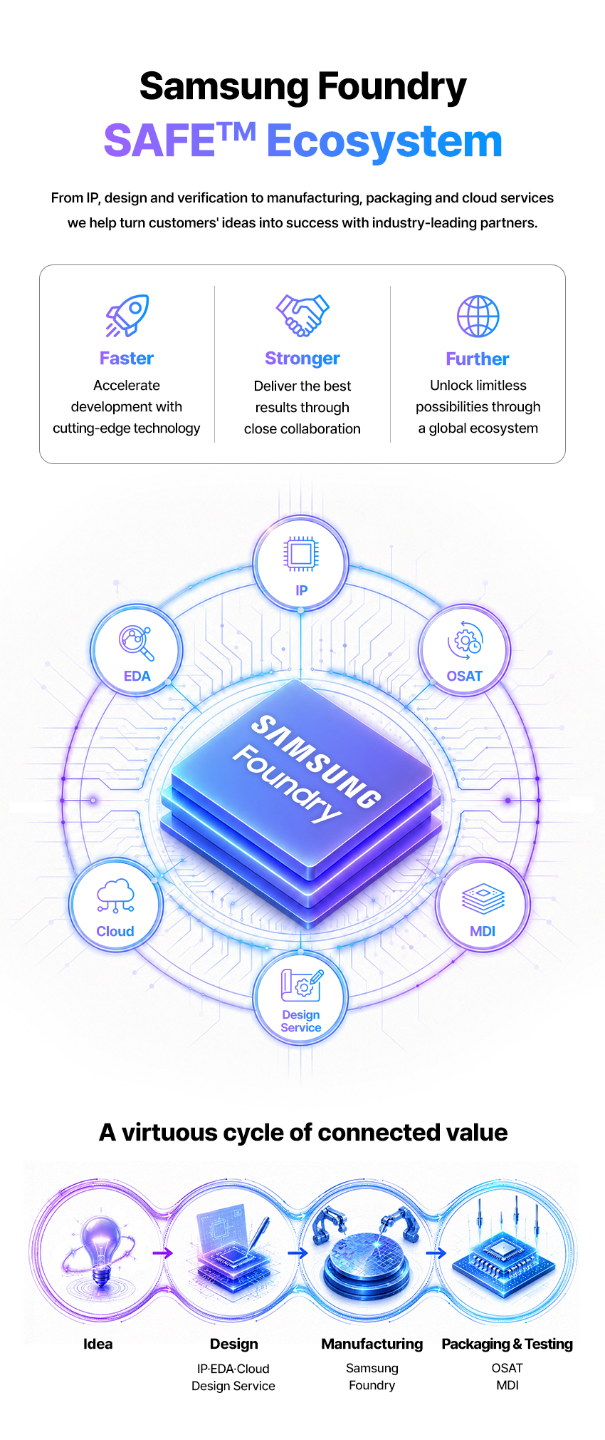
SAFE™ is Samsung Foundry’s collaborative ecosystem that connects customers, partners and technologies across every stage of semiconductor development, from chip design to mass production.
When a fabless customer brings an idea for a new chip, SAFE™ provides access to the partners and technologies needed throughout the development process. From IP selection and design tool validation to prototype production, packaging and testing, customers can find the expertise they need within a single integrated network.
Today, the SAFE™ ecosystem consists of six specialized alliances.
The Six SAFE™ Alliances: Bringing Industry Leaders Together Under One Ecosystem
① IP Alliance — Accelerating Development with Proven Design IP
Just as construction projects become more efficient by using prefabricated building materials, semiconductor development can be accelerated by using pre-verified design blocks. The IP Alliance provides these proven design assets, helping reduce both development time and risk.
The alliance offers a broad portfolio of semiconductor IP, including USB interfaces, memory controllers and CPU cores widely used in mobile, high-performance computing (HPC), AI and automotive applications. By providing these proven design blocks, the IP Alliance enables fabless companies to accelerate development without having to design every circuit from scratch.
Since Samsung Foundry launched the SAFE™ program, the number of IP partners has grown to more than 50 companies, with a portfolio of approximately 5,300 IP assets.
② EDA Alliance — Optimizing Design Tools for Samsung’s Process Technologies
Even the best chip design cannot be manufactured successfully if the design tools are not fully optimized for the target process technology. The EDA Alliance ensures that chip design software is fully validated and optimized for Samsung Foundry’s process technologies.
Working with leading EDA companies, Samsung provides certified design tools and methodologies for chip verification. Through its proprietary SAFE™ Qualified EDA (QEDA) certification program, Samsung verifies that EDA solutions meet its rigorous process requirements before they are used in customer projects.
This helps customers minimize design risks when adopting new process technologies while improving design quality and manufacturing reliability.
③ Cloud Alliance — Enabling On-Demand Design Environments
Building and maintaining semiconductor design infrastructure requires a significant investment. The Cloud Alliance enables customers to securely access Samsung Foundry’s design platform without having to build and maintain their own infrastructure.
Working with leading cloud service providers and EDA companies, Samsung enables customers to securely access its process design kits, design tools and development environment through the cloud.
This cloud-based approach reduces infrastructure costs, shortens development cycles and improves collaboration efficiency.
④ Design Solution Alliance (DSA) — Supporting Customers with Limited Design Experience
For fabless companies with innovative ideas but limited design experience, the Design Solution Alliance (DSA) connects them with experienced partners that support the entire chip design process.
Working with Design Solution Partners (DSPs) and Virtual Design Partners (VDPs), Samsung Foundry provides end-to-end design services, from design optimization and verification to tape-out, the final stage before manufacturing begins.
⑤ Multi-Die Integration (MDI) Alliance — Advanced Packaging for Multi-Chip Integration
Instead of integrating every function into a single chip, today’s AI and HPC semiconductors increasingly combine multiple chips with different functions into a single package. This approach improves both performance and power efficiency beyond what a single chip can achieve.
The Multi-Die Integration (MDI) Alliance brings together partners across design, IP, packaging and testing to support multi-chip integration within a single package. This includes both 2.5D packaging, in which chips are placed side by side on an interposer and 3D packaging, where chips are stacked vertically.
In collaboration with EDA, IP, DSP and OSAT partners, the MDI Alliance optimizes 2.5D and 3D packaging technologies, providing seamless, comprehensive solutions from initial design through packaging.
⑥ OSAT Alliance — One-Stop Assembly and Testing
Chip manufacturing does not end when wafer fabrication is complete. The individual chips must be diced, packaged and tested before they become finished products.
The Outsourced Semiconductor Assembly and Test (OSAT) Alliance brings together leading OSAT partners to provide one-stop assembly and testing services.
By integrating assembly and testing processes, Samsung helps accelerate the commercialization of advanced 2.5D and 3D packaged products optimized for HPC, mobile and automotive applications.
Supporting Ecosystem Partners
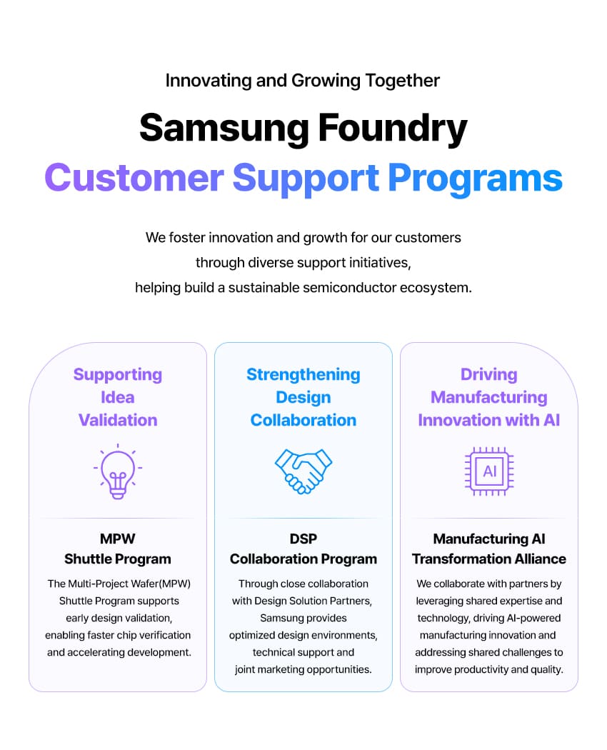
A thriving ecosystem is built on more than its structure alone. Samsung Foundry operates a range of support programs to help ecosystem partners and customers grow together.
These programs are not sequential steps in the design process. Instead, they are independent support initiatives that customers can use individually or in combination, depending on their specific needs.
MPW Shuttle Program — Lowering the Cost Barrier to Prototype Development
One of the biggest barriers for emerging fabless companies is the high cost of developing prototypes.
Samsung Foundry’s Multi-Project Wafer (MPW) Shuttle Program places designs from multiple companies on a single wafer, allowing them to share mask costs. This enables fabless companies to validate new ideas more efficiently and cost-effectively.
Samsung Foundry continues to expand the program, making advanced process technologies more accessible to small and mid-sized fabless companies.
DSP Collaboration — Bridging the Design Capability Gap
For fabless companies with innovative ideas but limited experience in advanced process design, collaboration with design houses is a key source of support.
Samsung Foundry works closely with its EDA, IP and DSP partners to provide process support, design kits, IP and design services.
The goal is to seamlessly bridge the gap between concept and creation, ensuring customer-centric fabless designs are successfully brought to market through Samsung Foundry’s advanced manufacturing.
Building a Virtuous Cycle
Samsung envisions a virtuous cycle in which fabless companies develop products that meet customer demand, Samsung Foundry manufactures them at scale and the finished products are delivered to end customers, creating opportunities for growth not only for customers, but also for Samsung Foundry and its ecosystem partners. SAFE™ is the collaborative platform that brings this vision to life.
Through its six alliances and customer support programs, SAFE™ connects every stage of semiconductor development and production, from chip design to packaging. Together with support programs such as the MPW Shuttle Program and DSP collaboration, SAFE™ provides meaningful support for the continued growth of the system semiconductor ecosystem.
In the AI era, innovation can no longer be achieved through the technological capabilities of a single company alone. Competitiveness depends on building an ecosystem in which companies across the value chain are closely connected and work together.
As a platform that connects innovation with global partners, Samsung Foundry’s SAFE™ ecosystem will continue to play a central role in advancing the next generation of system semiconductors.
For more in-depth explanation of the SAFE™ program, please visit the Samsung Semiconductor on the official website.