The Invisible Highways: Tracing the Journey Inside a Semiconductor Fab


A sophisticated, automated transport network forms the hidden backbone of semiconductor manufacturing, covering vast distances with remarkable precision.
Inside the highly controlled, ultra-clean environment of a state-of-the-art fabrication plant (fab), each silicon wafer undergoes hundreds of complex processing steps. Although they may seem stationary to the eye, wafers are constantly on the move, carried seamlessly between tools by an advanced internal logistics system.
At the heart of this system is the Overhead Hoist Transport (OHT) network. These autonomous vehicles, gliding along ceiling-mounted tracks, are responsible for the rapid and precise delivery of wafers, housed in specialized pods called FOUPs, to each designated processing equipment. This carefully orchestrated automation ensures that each wafer receives the required treatments at the precise moment.
Putting the Scale in Perspective: Global Comparison
The cumulative distances covered by the OHT system are remarkable. To put this scale into perspective, consider how the journey compares with traveling between well-known global landmarks.
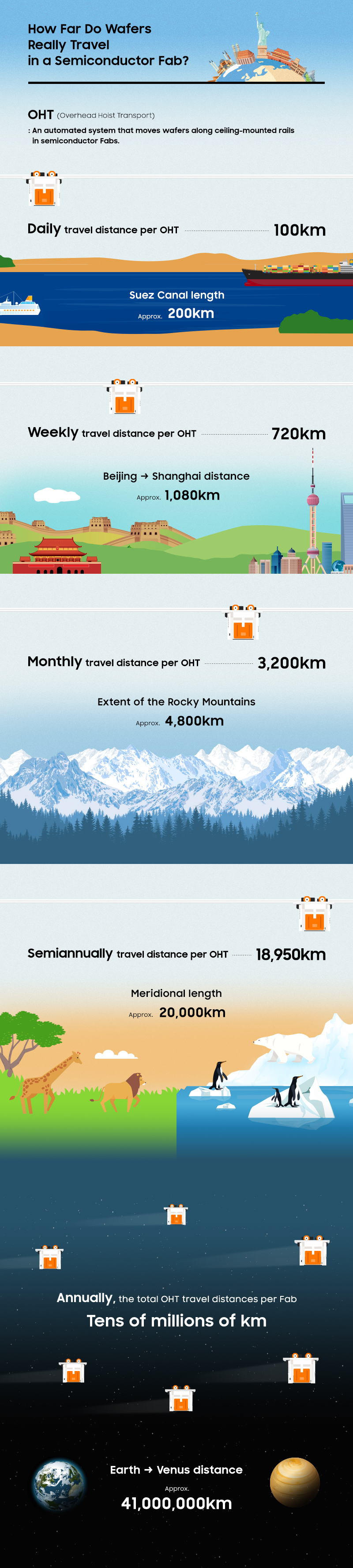
- Daily: A single OHT vehicle travels approximately 100 kilometers per day, comparable to the length of the Suez Canal.
- Weekly: The distance extends to roughly 720 kilometers per week, similar to a trip from Beijing to Shanghai.
- Monthly: Over a month, one vehicle covers 3,200 kilometers, nearly matching the full length of the Rocky Mountains in North America.
- Semiannually: Every six months, a singly OHT vehicle covers around 18,950 kilometers, nearly matching Earth’s meridional length
- Annually: Across a year, the total OHT travel distance in a single fab reaches tens of millions of kilometers, almost enough for a journey from Earth to Venus.
The extraordinary distances highlight the vast scale of automation and precision logistics required for modern chipmaking. This silent, continuous flow of wafers is a critical element in transforming raw silicon into the foundational technology of the 21st century.