Samsung Foundry 4nm FinFET: The Best of Both Worlds for Performance and Reliability


One of the hardest decisions in semiconductor design is choosing between cutting-edge and proven process nodes. Leading-edge processes deliver top-tier performance, but early production runs can bring unexpected variables. More established processes offer rock-solid reliability, yet often leave something to be desired on the performance side.
Samsung Foundry’s 4nm FinFET process strikes an ideal balance between these two extremes.
A Process Where Experience Is the Edge
The 4nm process has been refined through years of high-volume manufacturing. That accumulated experience translates directly into lower defect rates and more consistent quality. Think of it like a well-worn engine that’s had every rough edge smoothed out — the longer a process runs at scale, the more predictable and dependable it becomes.
For the companies building chips on this process, that predictability is everything. It means knowing exactly how many chips will come off the line, what they’ll cost, and when they’ll be ready — with confidence.
More Freedom for Designers. Better Devices for Everyone.
Another defining strength of the 4nm process is flexibility. Within a single process node, designers can tune their chips in very different directions depending on what the end product demands.
When performance is the priority: Ultra-low Vth (uLVT) option enables faster switching speeds, pushing computational power to its limits. Ideal for gaming chips, AI inference engines and high-performance computing.
When battery life matters more: High Vth (HVT) option reduces leakage current, cutting standby power consumption — a meaningful win for wearables and other devices that need to last through the day.
The internal wiring architecture has also been redesigned, reducing signal delay across the chip by roughly 26%. It’s a change you’ll never see, but one you’ll feel — in faster responses, smoother performance and better efficiency.
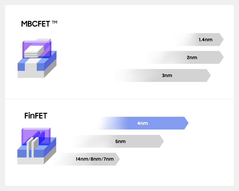
The Pinnacle of FinFET — and a Foundation for What’s Next
The 4nm FinFET represents the most refined evolution of Samsung’s FinFET architecture, developed right at the threshold of the transition to next-generation GAA technology. That maturity makes it broadly capable across industries — from AI and memory to automotive and RF communications, each with its own demanding set of requirements.
A process this mature doesn’t just perform well. It gives designers the confidence and flexibility to build better products. That’s why 4nm FinFET remains one of the most compelling choices in Samsung Foundry’s portfolio today.
Powering the Future: From AI to Network
Because the 4nm process is so versatile, it serves as the hidden engine for some of the world’s most advanced technologies:

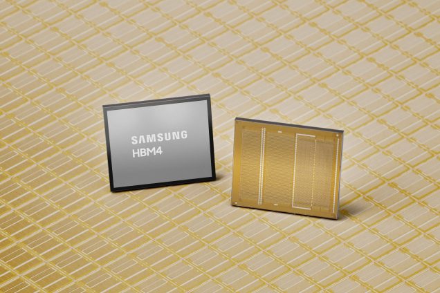
- HBM: Optimizing Power and Thermal Efficiency
HBM4 demands extremely high bandwidth for large-scale data transfer while operating in constrained spaces, where managing power and heat is critical. The 4nm process minimizes power loss through low-voltage operation and low-resistance interconnects, enabling highly efficient designs even in dense integration scenarios. Samsung’s HBM4 base die, which entered mass production in February, is built on its 4nm process.
- AI/HPC: Enabling Large Die and Yield Scalability
AI requires massive, complex chips to process human language and logic. The 4nm process handles these large-scale “brains” with ease, ensuring high-speed data processing while keeping power consumption in check.
A leading U.S. company’s LPU (Language Processing Unit), built on a large die architecture, utilizes the 4nm process to achieve both high-density interconnects and power efficiency. It meets stringent requirements for power delivery stability and thermal management while supporting high-speed data processing, demonstrating the maturity of the platform.
- Smart Cars: High Performance Under Power Constraints
The cars of tomorrow, featuring advanced autonomous driving, are basically supercomputers on wheels. Samsung’s 4nm tech provides the massive computational power these cars need to navigate safely, all while operating under the strict battery and heat constraints of a vehicle.
- Next-Gen Connectivity: Built for Speed and Efficiency
As we move toward the future of ultra-fast Wi-Fi 8 and 6G networks, communication chips must process complex signals efficiently. The 4nm process reduces power consumption, while ensuring high-speed, stable connectivity.
A Scalable Platform Built on Proven Maturity
Samsung Foundry’s 4nm process is the pinnacle of its kind — the final, most perfected evolution of the FinFET architecture.
By delivering a solution that is simultaneously powerful, energy-efficient and incredibly reliable, Samsung is providing the foundational building blocks for the next generation of technology.
In the end, Samsung’s 4nm FinFET isn’t just about smaller chips. It’s about delivering the reliable performance and efficiency that next-generation AI, automotive and high-performance computing systems depend on.
For more information on the technologies applied to Samsung Electronics’ 4nm process and its application-specific characteristics, please visit the Samsung Semiconductor Tech Blog on the official website.