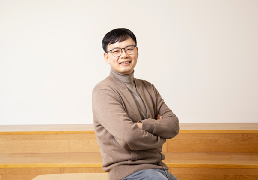
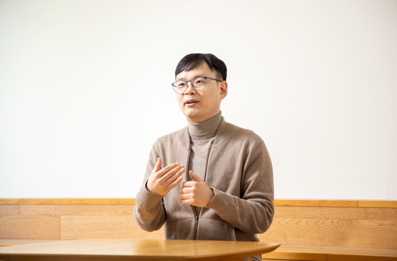
Samsung Electronics’ Kee‑Bong Song and Jin-Woo Han Named IEEE Fellows
Samsung Electronics announced that Dr. Kee‑Bong Song, Senior Vice President and Head of the System LSI Research Center at Samsung Device Solutions Research America (DSRA), and Dr. Jin-Woo Han, Vice President of the DRAM TD Team at Samsung’s Semiconductor Research Center, have been elevated to IEEE Fellow, Class or 2026 by the Institute of Electrical and Electronics Engineers (IEEE).
The IEEE Fellow distinction is the organization’s highest membership grade and is awarded annually to fewer than 0.1% of IEEE members worldwide who have demonstrated exceptional technical achievements and contributions to industry and society. This recognition highlights the two researchers’ longstanding leadership and sustained contributions in next-generation communications and memory technologies.
Recognized for Contributions to 5G Modem and NTN Technologies
With extensive experience across global technology companies, Dr. Song currently leads System LSI research at Samsung’s U.S. R&D Center, overseeing work in modems, connectivity, on-device AI, and system-on-chip (SoC) technologies. He has published extensively in wireless communications, signal processing, and AI-assisted modem-RF systems, and holds more than 80 patents.
His elevation to IEEE Fellow recognizes his contributions to cellular modem-RF system design and performance optimization, including the industry’s first 5G modem development, advancements in 5G millimeter-wave (mmWave) transceiver technologies, and the commercialization of Non-Terrestrial Network (NTN)-based services. These technologies enabled features such as Satellite SOS, implemented in products including the Exynos Modem 5400 and Exynos 2500.
* NTN (Non-Terrestrial Networks) refers to mobile communication networks that use satellites to provide coverage in remote areas or emergency situations.
Samsung Semiconductor Newsroom spoke with Song about the significance of the recognition and his outlook on future research directions.

Q. Congratulations on being named an IEEE Fellow for 2026. How do you feel about this recognition?
I am honored that the technologies and products I have developed as a researcher and engineer, together with colleagues at at Samsung’s global R&D teams and partners, have been recognized for their contributions to society. I am deeply grateful for the support of my research and development teammates and Samsung’s leadership.
Q. Being selected as an IEEE Fellow carries special significance. What does this appointment mean to you personally?
This recognition is particularly meaningful to me. My former advisor at Stanford University, Professor John M. Cioffi, nominated me for Fellow, and being acknowledged as a technologist who has lived up to that trust is truly an honor.
When I first heard the news, it didn’t feel real. I have followed the paths laid by many outstanding innovators before me, learning from their guidance and support. Moving forward, I hope to continue contributing to society through the development of advanced semiconductor technologies and products.
Q. Looking ahead, what technology areas will DSRA focus on?
In the era of 6G and Physical AI, data generated by machines and sensors will increasingly interact. We aim to create new semiconductor technologies and products at the intersection of communication, compute, and sensing, and to help drive future innovation.
* Physical AI: AI that interacts with the physical world through sensors and machines

Q. Is there a message you would like to share with semiconductor researchers in Korea and around the world?
As the 6G and Physical AI era unfolds, the role and potential of system semiconductors will continue to expand. I have great respect for researchers who pursue innovation with passion in their respective fields. I look forward to collaborating with many researchers to advance system semiconductor technologies that contribute to society and help protect lives.
Recognized for Leadership in Next-Generation 3D DRAM Research
Jin-Woo Han has led research into next-generation 3D DRAM technologies aimed at overcoming the limits of conventional DRAM scaling. By stacking DRAM cells vertically rather than arranging them solely in a planar structure, this approach enables higher memory density per chip area and is considered a key direction for future memory technologies.
After working at NASA, Han joined Samsung Electronics and has since accumulated more than 200 patents and published over 160 SCI-indexed papers across memory, logic, and sensor technologies. His IEEE Fellow appointment recognizes his contributions to 3D DRAM development and decades of sustained research achievements.
Han shared his insights on the future of DRAM technology with Samsung Semiconductor Newsroom.

Q. Congratulations on being named an IEEE Fellow for 2026. What does this recognition mean to you?
Day to day, not much has changed, but personally, the recognition carries great significance. IEEE Fellows are selected through nomination and evaluation by existing Fellows, and I am grateful that my publications, conference activities, and service to the academic community were positively assessed. Being recognized by fellow researchers is a great honor.
Q. How does 3D DRAM differ from conventional DRAM architectures?
In simple terms, it mirrors the evolution of flash memory in the early 2010s, when planar structures transitioned to vertically stacked V-NAND. Traditional DRAM increased density by packing cells more tightly on a planar surface, but continued scaling led to fundamental challenges such as leakage current and cell-to-cell interference.
3D DRAM addresses these limitations by enlarging individual cell dimensions to restore electrical characteristics, increasing spacing between cells to reduce interference, and stacking cells vertically to expand capacity per chip area. DRAM using this vertical stacking approach is referred to as VS-DRAM (Vertically Stacked DRAM).
Q. As head of next-generation DRAM research, what technologies will you focus on going forward?
Looking back at the history of semiconductors, two trends stand out: breakthrough technologies that overcame scaling limits, and innovations that reduced chip costs. Today, the widespread adoption of AI has created new opportunities to increase the value of data.
In this context, I am focusing on wafer bonding as a key enabling technology. It provides the foundation for implementing 3D structures that allow fast and reliable interconnection of signals across multiple memory layers.
Q. Do you have any advice for semiconductor researchers currently pursuing their work?
Korea’s semiconductor industry has built global leadership through strong competitiveness in commodity products. However, rapid changes in the global supply chain and intensifying technology competition present both risks and opportunities.
As demand for customized specialty products continues to grow, researchers will benefit from a broad understanding of related technologies as well as deep insight into product structures and hierarchies. Taking a global perspective and building collaborative international research networks will also be critical to future competitiveness.
Their elevation to IEEE Fellow underscores global recognition of Korea’s semiconductor technologies. Samsung Electronics will continue advancing semiconductor innovation through close collaboration with researchers worldwide, shaping technologies for the next era.