Samsung Electronics Holds Memory Tech Day 2023 Unveiling New Innovations To Lead the Hyperscale AI Era


Event spotlights next-generation memory solutions for applications such as cloud, edge devices and automotive vehicles
New technologies and products include HBM3E Shinebolt, LPDDR5X CAMM2
and Detachable AutoSSD to accelerate innovation for future computing requirements
.
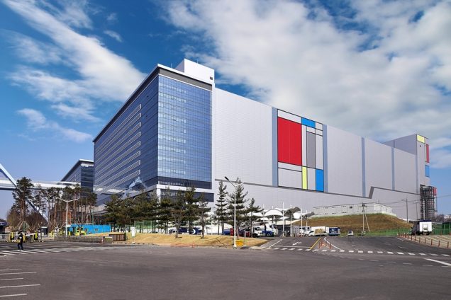
SAN JOSE, Calif. – October 20, 2023 – Samsung Electronics Co., Ltd., a world leader in advanced memory technology, today held its annual Memory Tech Day, showcasing industry-first innovations and new memory products to accelerate technological advancements across future applications — including the cloud, edge devices and automotive vehicles.
Attended by about 600 customers, partners and industry experts, the event served as a platform for Samsung executives to expand on the company’s vision for “Memory Reimagined,” covering long-term plans to continue its memory technology leadership, outlook on market trends and sustainability goals. The company also presented new product innovations such as the HBM3E Shinebolt, LPDDR5X CAMM2 and Detachable AutoSSD.
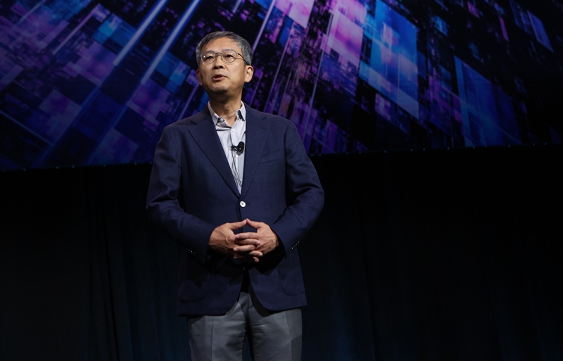
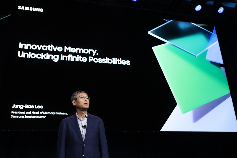
Jung-Bae Lee, President and Head of Memory Business at Samsung Electronics, used his keynote address to expand on how Samsung will overcome the challenges of the hyperscale era through innovations in new transistor structures and materials. For example, Samsung is currently preparing new 3D structures for sub-10-nanometer (nm) DRAM, allowing larger single-chip capacities that can exceed 100 gigabits (Gb). Following its 12nm-class DRAM that began mass production in May, 2023, Samsung is working on its next-generation 11nm-class DRAM, which is set to offer the industry’s highest density.
NAND flash breakthroughs that will shrink cell sizes and refine channel hole etching techniques are also in development, with the goal of ushering in 1,000-layer vertical NAND (V-NAND). Development is on track for Samsung’s ninth-generation V-NAND to provide the industry’s highest layer count based on a double-stack structure. The company has secured a functional chip for the new V-NAND and plans to start mass production early next year.
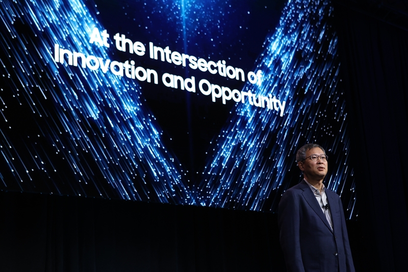
“The new era of hyperscale AI has brought the industry to a crossroads where innovation and opportunity intersect, presenting a time with potential for great leaps forward, despite the challenges,” said Lee. “Through endless imagination and relentless perseverance, we will continue our market leadership by driving innovation and collaborating with customers and partners to deliver solutions that expand possibilities.”
.
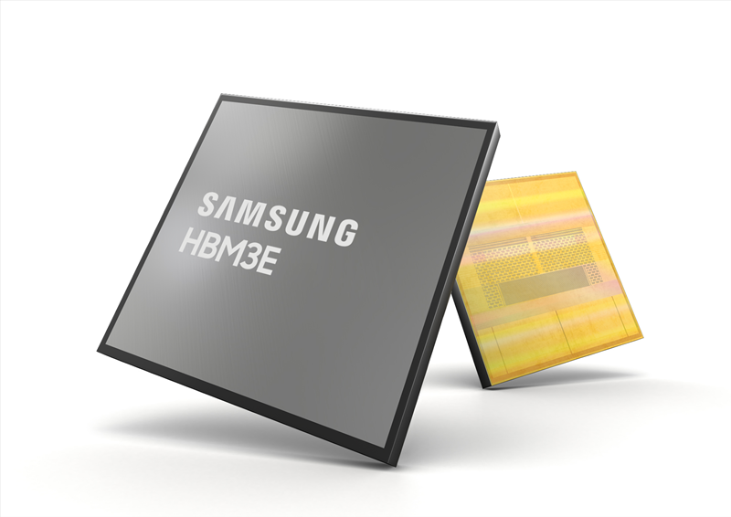
Introducing HBM3E ‘Shinebolt’
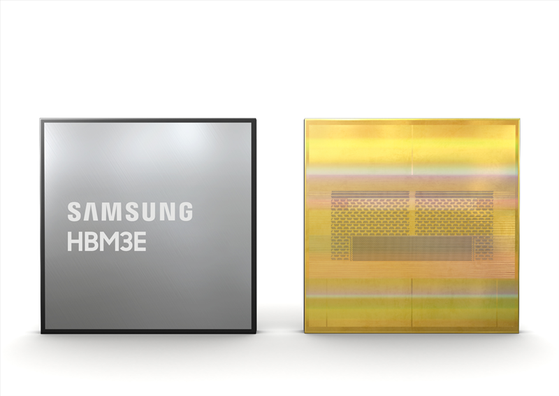
Today’s cloud systems are evolving to optimize compute resources, which require high-performance memory to handle high capacity, bandwidth and virtual storage capabilities. Building on Samsung’s expertise in commercializing the industry’s first HBM2 and opening the HBM market for high-performance computing (HPC) in 2016, the company today revealed its next-generation HBM3E DRAM, named Shinebolt.
Samsung’s Shinebolt will power next-generation AI applications, improving total cost of ownership (TCO) and speeding up AI-model training and inference in the data center. The HBM3E boasts an impressive speed of 9.8 gigabits-per-second (Gbps) per pin speed, meaning it can achieve transfer rates exceeding up to more than 1.2 terabytes-per-second (TBps).
In order to enable higher layer stacks and improve thermal characteristics, Samsung has optimized its non-conductive film (NCF) technology to eliminate gaps between chip layers and maximize thermal conductivity.
Samsung’s 8H and 12H HBM3 products are currently in mass production and samples for Shinebolt are shipping to customers. Leaning into its strength as a total semiconductor solutions provider, the company also plans to offer a custom turnkey service that combines next-generation HBM, advanced packaging technologies and foundry offerings together.
Other products highlighted at the event include the 32Gb DDR5 DRAM with the industry’s highest capacity, the industry’s first 32Gbps GDDR7 and the petabyte-scale PBSSD, which offers a significant boost to storage capabilities for server applications.
.
Redefining Edge Devices Through Powerful Form Factors
In order to process data-intensive tasks, today’s AI technologies are moving toward a hybrid model that allocates and distributes workload among cloud and edge devices. Accordingly, Samsung introduced a range of memory solutions that support high-performance, high-capacity, low-power and small form factors at the edge.
In addition to the industry’s first 7.5Gbps LPDDR5X CAMM2[1] — which is expected to be a true game changer in the next-generation PC and laptop DRAM market — the company also showcased its 9.6Gbps LPDDR5X DRAM, LLW[2] DRAM specialized for on-device AI, next-generation Universal Flash Storage (UFS), and the high-capacity Quad-Level Cell (QLC) SSD BM9C1 for PCs.
.
Paving the Road for Automotive Memory Solutions Leadership
With advancements in autonomous driving solutions, market demand is also rising for high-bandwidth, high-capacity DRAM and Shared SSDs, which share data with multiple System on Chips (SoCs). Samsung presented its Detachable AutoSSD that allows data access from a single SSD to multiple SoCs through virtual storage.
The Detachable AutoSSD supports sequential read speed of up to 6,500 megabytes-per-second (MBps) with 4TB of capacity. As it comes in a detachable form factor, the SSD makes upgrades and adjustments easier for vehicle users and manufacturers. Samsung also displayed automotive memory solutions such as high-bandwidth GDDR7 and LPDDR5X with a more compact package size.
.
Technology That Makes Technology Sustainable
As part of its commitment to minimizing environmental impact, Samsung underscored a variety of innovations within its semiconductor operations that will contribute to increased energy efficiency for customers and consumers.
The company plans to secure ultra-low-power memory technologies that can decrease power consumption in data centers, PCs and mobile devices, while using recycled materials in portable SSD products to reduce its carbon footprint. Samsung’s next-generation solutions, such as the PBSSD, will also help reduce energy usage for server systems as they maximize space efficiency and rack capacity.
While collaborating with stakeholders across the semiconductor value chain, including customers and partners, Samsung’s semiconductor business will continue to play an active role in tackling global climate issues through its sustainability initiative, “technology that makes technology sustainable.”
To learn more about Samsung Semiconductor’s solutions and Samsung Memory Tech Day 2023, please visit: https://semiconductor.samsung.com/events/techday-memory-2023/. The recap of the event will be posted at a later date.
[1] CAMM: Compression Attached Memory Module.
[2] LLW: Low Latency Wide I/O.
Related tag
#Detachable AutoSSD
#HBM3E Shinebolt
#LPDDR5X CAMM2
#Memory Reimagined
#Memory Tech Day
#Memory Tech Day 2023
#NAND flash