Samsung and Its Foundry Partners Reveal Solutions for a Strong Design Infrastructure at SAFE Forum 2021


San Jose, California, USA — November. 17, 2021 — Samsung Electronics, a world leader in advanced semiconductor technology, held its 3rd Annual Samsung Advanced Foundry Ecosystem (SAFETM) Forum 2021 virtually today.
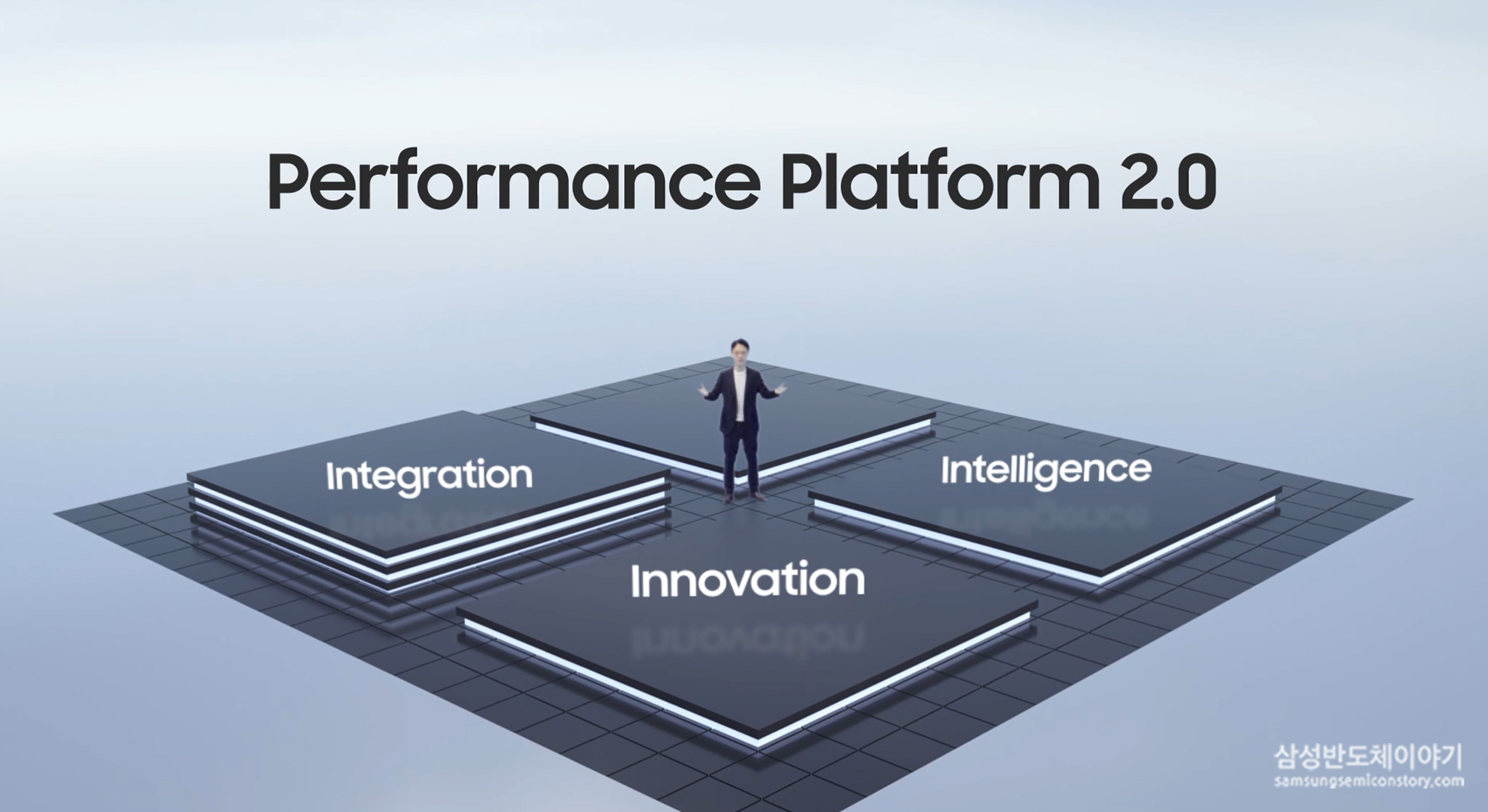
With the theme of ‘Performance Platform 2.0: Innovation, Intelligence, Integration’, Samsung and its foundry ecosystem partners prepared 7 plenary talks and 76 technology sessions focused on three main topics: Gate-All-Around (GAA, Innovation), Artificial Intelligence (AI, Intelligence), and 2.5D/3D (Integration) technologies and the diverse design infrastructures required for high-performance applications.
“In the rapidly changing data-centric era, Samsung and its foundry partners have made great strides responding to increasing customers demand and to support their success by providing powerful solutions,” said Ryan Lee, Senior Vice President and Head of Foundry Design Platform Development at Samsung Electronics. “With the support of our SAFE program, Samsung will lead the realization of the vision ‘Performance Platform 2.0’.”
Starting with a keynote live streaming on November 17, attendees are able to explore a variety of tech sessions and engage with ecosystem partners through the virtual SAFE Forum platform for a month. To register for SAFE forum, please visit https://www.samsungfoundry.com
SAFE 2021: Performance Platform 2.0
Samsung has concentrated on expanding its foundry ecosystem by focusing on IP, Electronic Design Automation (EDA), Cloud, Design Solution Partner (DSP), and Package solutions necessary for today’s data-driven era. Samsung introduced today its latest SAFETM program including:
SAFE™-IP & EDA: Samsung and its foundry ecosystem have reserved over 3,600 IPs and 80 certified EDA tools respectively. These are developed and verified based on the high-standard of certification program run by Samsung and participated in by our partners. In order to respond to the demands of high performance applications, Samsung’s foundry ecosystem has developed not only HPC-specific foundation IPs including standard cell libraries and memory compilers but also key IPs, such as over 100Gbps Serializer-Deserializer (SerDes) interface and 2.5D/3D multi-die integration solutions.
With our EDA partners, Samsung has secured design tools optimized for its unique 3-nanometer (nm) GAA process technology and design methodology for integrating multiple dies in 2.5D/3D. Customers can also utilize AI- and machine learning- based EDA technology to systematically manage and analyze design data. To overcome the increasing difficulties of chip design and analysis, Samsung has strengthened cooperation with partners to develop EDA tools and related technologies, such as incorporating GPUs that can efficiently use computing resources required for chip verification.
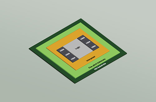
SAFE™-OSAT: Samsung plans to lead ‘beyond-Moore’ technologies by strengthening various package line-ups such as 2.5D/3D through the expansion of its SAFE-Outsourced Semiconductor Assembly and Test (OSAT) ecosystem. The recent announcement of the co-development of Hybrid-Substrate Cube (H-Cube) solution, which offers efficient integration of 6 HBMs and cost benefit, is one of the successful examples of Samsung foundry’s collaboration with the OSAT community.
SAFE™-Cloud Design Platform: SAFE™-CDP, the cloud-based one-stop design platform introduced last year, now supports a hybrid cloud function that can be linked to customers’ conventional design environments.
SAFE™-DSP: Through the SAFE™-DSP ecosystem, Samsung and its global partners can actively support global fabless companies to implement their design ideas into custom product by utilizing cutting-edge process technologies as well as high-performance, low-power chip design knowledge.
Quote from SAFETM Partner companies
- Ansys, Ajei Gopal, CEO
“Today’s chips demand a full multiphysics approach, which requires engineering simulation. Ansys is proud to partner with Samsung to deliver a comprehensive multi-physics analysis flow for Samsung’s multi-die integration initiative. The benefits to joint customers, to the industry – and to the entire world – are tremendous. Semiconductors will drive innovations as varied as autonomous and electric vehicles, artificial intelligence, and mobile technologies, including 5G and beyond.”
- Arm, Simon Segars, CEO
“Our longstanding partnership with Samsung Foundry has been essential for growing business opportunities in many markets for our combined partner ecosystem. This close collaboration continues as we work together to optimize our Armv9 next-generation processors on Samsung Foundry’s leading-edge processes, including GAA, to deliver a best-in-class solution that is optimized for the world of today, and the technologies of tomorrow. Together, we are unlocking new opportunities across HPC, Automotive, AI, and IoT, while also managing rising complexities, enabling faster time to market.”
- Cadence, Lip-Bu Tan, CEO
“The Cadence Intelligent System Design strategy is very well-aligned with Samsung Foundry’s Performance Platform 2.0 with common themes of innovation, pervasive intelligence and integrated solutions. Together, we’re enabling customers to develop and deliver innovative, breakthrough products using Samsung’s most advanced process and packaging technologies, and we look forward to continuing our work with Samsung Foundry to accelerate design successes”
- Siemens EDA, A.J.Incorvaia, Senior Vice President
“Quo The Samsung SAFE event provides an exceptionally valuable venue for the Samsung Foundry ecosystem to meet, share information and identify opportunities to fully leverage Samsung’s cutting-edge process technologies. Siemens EDA looks forward to this year’s Samsung SAFE event and the many opportunities it presents for collaborating with customers and partners to eliminate design obstacles and enhance silicon success.”
- Synopsys, Sassine Ghazi, president and COO
“We see exciting times ahead as software and chip technology come together to create world-changing new products,” said Sassine Ghazi, president and COO of Synopsys. “We have strong programs with Samsung Foundry on 3nm gate-all-around enablement, broad IP certification, AI-assisted chip design and 2.5/3D multi-die design to name just a few. We welcome the strong collaboration opportunities offered by the Samsung SAFE initiative.”