Inside the Chip: The Fascinating Journey of Semiconductor Manufacturing – Part 4


Metal Wiring: Laying out Electrical Highways
After the ion implantation process, we now have a wafer with semiconductor properties, which can be made to conduct or insulate electrical current as needed. Repeating the photolithography, etching, and ion implantation steps creates numerous semiconductor circuit layers on the wafer. For these to work, an electrical signal must be applied from the outside and then transmitted along the network of circuits. This is where metal interconnects are needed to be laid out as highways for the electrical signals to travel.
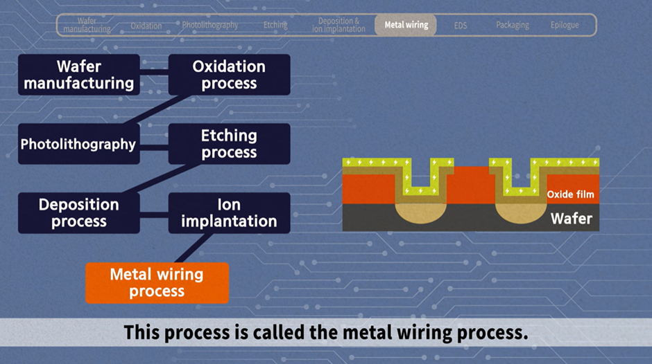
Metal wiring is a process of forming reliable and efficient interconnects across multiple layers of the chip. The process utilizes the conductive properties of metals through which electrical signals can freely flow, but not all metals can be used. To qualify for use in semiconductor chips, metals must satisfy certain conditions such as wafer adhesiveness, low electrical resistance, thermal and chemical stability and high reliability. Metals which are commonly used include aluminum (Al), copper (Cu), and tungsten (W).
The laying of metal wires is also carried out using a deposition process. A metal is placed in a vacuum chamber and boiled or electrically shocked at low pressure, which turns the metal into a gas. The wafer is placed in the vacuum chamber, and a thin metal film is formed on the wafer.
EDS: Ensuring Perfection
Once the wafer fabrication (FAB) is complete, the wafer enters the EDS, or Electrical Die Sorting, process. In short, EDS is a quality control phase where each chip is tested to ensure it functions as intended. As the name suggests, electrical characteristics are tested to make sure each individual chip has reached the desired quality level.
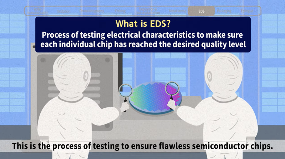
EDS is important in many different reasons. First, by sorting out defective chips at the wafer level, subsequent processing of such chips can be prevented, therefore increasing efficiency and reducing cost. Second, by identifying defects and problems, EDS provides data and feedback so that the issues in design or fabrication can be discovered and corrected. Lastly, the whole process eventually leads to increase in yield. Yield refers to the percentage of functional chips on a wafer and is a critical metric in the semiconductor manufacturing industry.
Packaging: Connecting to the System
We’ve reached the final part of our series, the ‘packaging’ process, which every chip must go through to function as a semiconductor in various electronic devices.
The wafer completed through the previous steps are cut into individual semiconductor chips. Each of these individually cut chips is called a bare chip or a die. However, at this stage, the chip is unable to exchange electrical signals with the outside and is vulnerable to damage from external impact. The aim of packaging is to connect the integrated circuit inside the chip to an electronic system and also to protect the circuits from external elements: high temperatures, high humidity, chemical agents, impact, and vibration.
So, how is it done? The packaging process involves enclosing the chip within a protective casing and making electrical connections to the electronic devices.
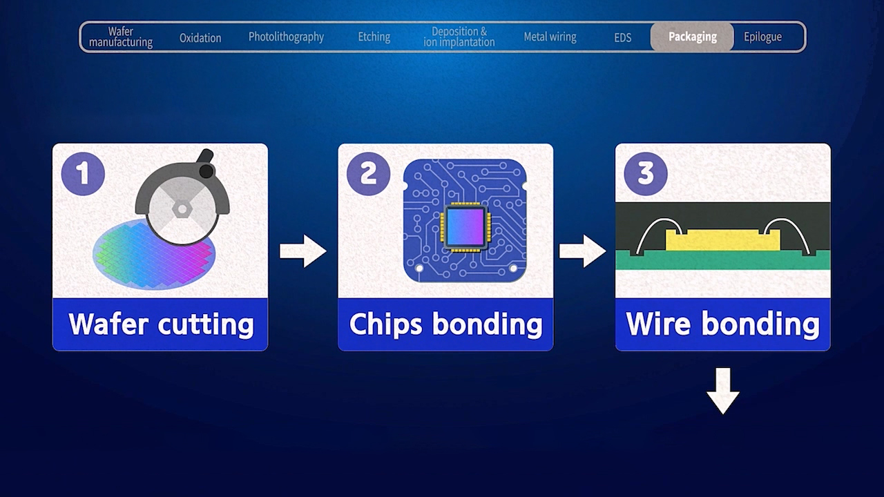
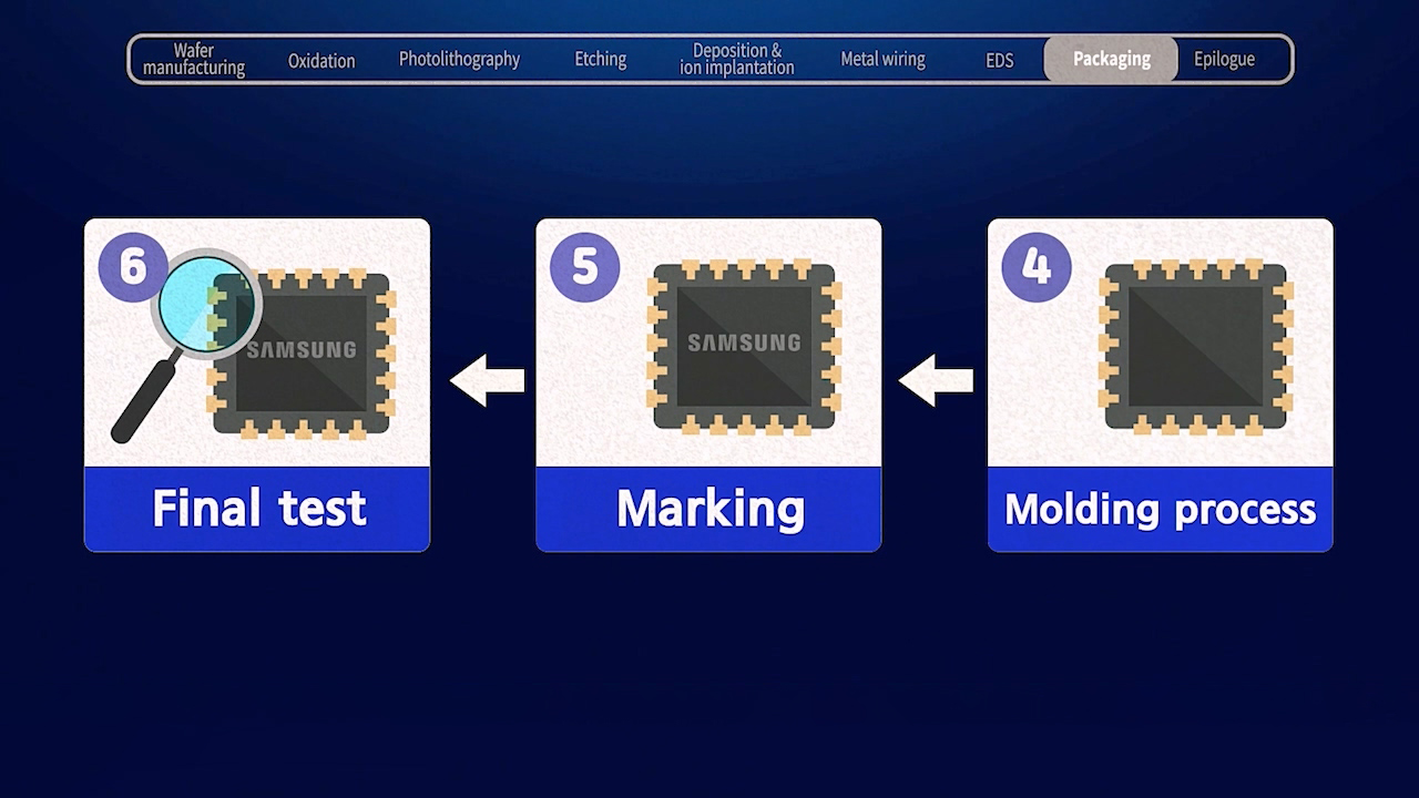
First, wafers completed through fabrication are cut into individual chips using a diamond saw or laser beams. These diced or sawn chips are then moved and attached onto a lead frame or printed circuit board (PCB), which works as a frame that protects and supports the chips, as well as transmitting electrical signals between the semiconductor chip and external circuits. The chips are placed on a substrate, and the contact point of the chip are connected and bonded with the contact point of the substrate using thin wires that will impart electrical properties to the chip. Aside from the traditional wire bonding method, there is a packaging method called flip chip where the chip and substrate are connected using ball-shaped bumps. Lastly, molding finishes the chip package to its desired shape, and after sealing the semiconductor and labeling the product name, the semiconductor chip is completed.
Today, there are many different types of packaging technology, including through-silicon via (TSV), 2.5D and 3D packaging, fan-out packaging, multi-chip package (MCP), and system-in-package (SiP). All these advanced packaging techniques are designed to meet the demands of smaller, faster, and more energy-efficient electronic devices.
At long last, after packaging comes the test to finally sort out defective chips. The semiconductor chips are placed in a tester and subjected to various levels of voltages, temperatures, humidity and electrical signals to test the final products’ electrical properties, functional properties, and operating speed. The data from the tester is analyzed and fed back into the manufacturing or assembly processes, further improving product quality.
So far, we have explored the intricate processes of semiconductor manufacturing. Next time we tap our smartphone or boot up a laptop, let’s take a moment to recognize the microscopic marvel within. Each chip is a product of relentless innovation, precision, and the ever-evolving semiconductor technology R&D.
For a more detailed understanding, check out the accompanying video, which offers clear explanations with visual demonstrations.