Inside the Chip: The Fascinating Journey of Semiconductor Manufacturing – Part 3


In the previous article, we looked into photolithography and etching, the steps that build the cornerstones of semiconductors by forming circuit patterns on a wafer. As semiconductor chips consist of many complex, microscopic layers of patterns, the steps need to be repeated multiple times to stack the layers, which can be compared to constructing dozens of floors for a high-rise building.
After forming each layer, the process of covering it with a thin film should follow, in order to connect, protect and insulate the circuits. In this part, we delve into how these thin films are made, which is the essence of a step called deposition.
Deposition and Ion Implantation: Adding Functionality
Deposition is a highly precise series of processes that lay down and coat thin films onto the circuit layers multiple times. The term ‘thin film’ refers to a film that is 1 micrometer or thinner (µm, one-millionth of a meter), which is a molecular or an atomic level.
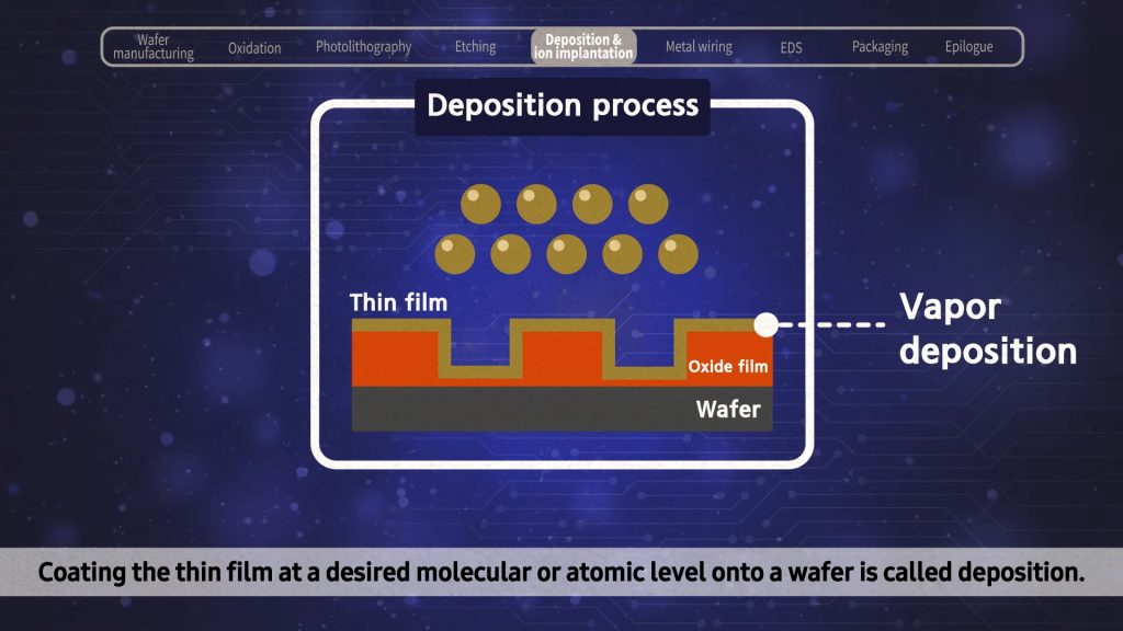
To accurately achieve this level of thickness and uniformly apply the thin film, two types of methods are used: physical vapor deposition (PVD) and chemical vapor deposition (CVD). While PVD deposits metal films and is not accompanied by chemical reaction, CVD ejects and deposits a vapor of particles formed by a chemical reaction of gas. The deposition process can be used to create thin films for different purposes, including a metal (conductive) layer which connects the electrical signals among the circuits and an insulating (dielectric) layer which prevents the flow of electric current.
Along with deposition, the task of giving the semiconductor electrical characteristics should be accompanied. This step is called ion implantation, because it is literally implanting ions into the wafer.
A semiconductor has both the characteristics of a conductor and an insulator (nonconductor), as we can assume by its name. A pure silicon wafer is an insulator and does not conduct electricity, but once ions of an element is added, the ions can alter the elemental composition of the target, given the ions differ in composition from the target. In this sense, ion implantation is the process that essentially turns a silicon wafer into a semiconductor, in other words imparting conductive properties and make the wafer able to conduct current.
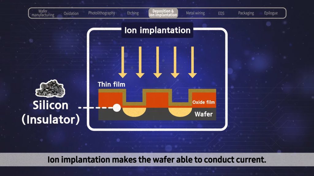
In the ion implantation process, the ions are turned into fine gaseous particles or ion beam, and then implanted into the front face of the wafer to the desired depth. The ions, called ‘impurities’ in semiconductor manufacturing, either come from Group 15 (phosphorus, P and arsenic, AS) or Group 13 (boron, B) on the periodic table. Implanting a Group 15 element gives an n-type semiconductor, while implanting a Group 13 element gives a p-type semiconductor.