Inside the Chip: The Fascinating Journey of Semiconductor Manufacturing – Part 2


In the previous article, we explored how wafers are made from silicon and how oxide films are formed on their surfaces as protective shields. Now, let’s dive into the next phase of semiconductor manufacturing: printing circuit patterns onto these wafers and building the actual circuits.
Photolithography: Drawing the Blueprint
Now, the actual construction of the circuits begins with a crucial step called photolithography. Much like drawing blueprints for a building, the purpose of the process is drawing a circuit design onto the wafer. The process, often simply called ‘photo’, is quite similar to developing a photo taken with a film camera.
There are a few key terms to understand before we dive into the procedure. First is ‘photoresist’, which is a light-sensitive material that undergoes a chemical reaction when exposed to light. Second is the ‘photomask’, a glass substrate with a computer-designed circuit pattern.
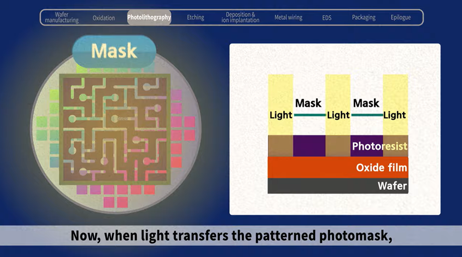
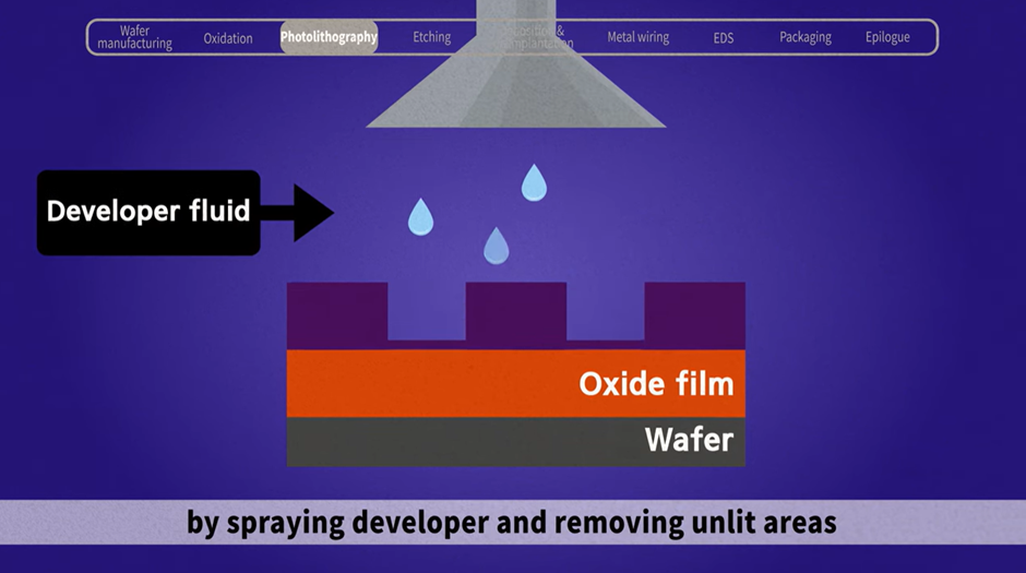
The process begins with evenly applying photoresist to the wafer’s surface, making it similar to photographic paper used for printing photos. Once the wafer is coated, a photomask is placed above it, and ultraviolet light goes through the photomask. As the light passes through the photomask, it exposes the desired pattern onto the photoresist layer on the wafer and selectively alters the properties of the exposed areas. After development, unlit areas are washed away, leaving the substrate with the imprinted circuit pattern.
Etching: Carving the Pathways
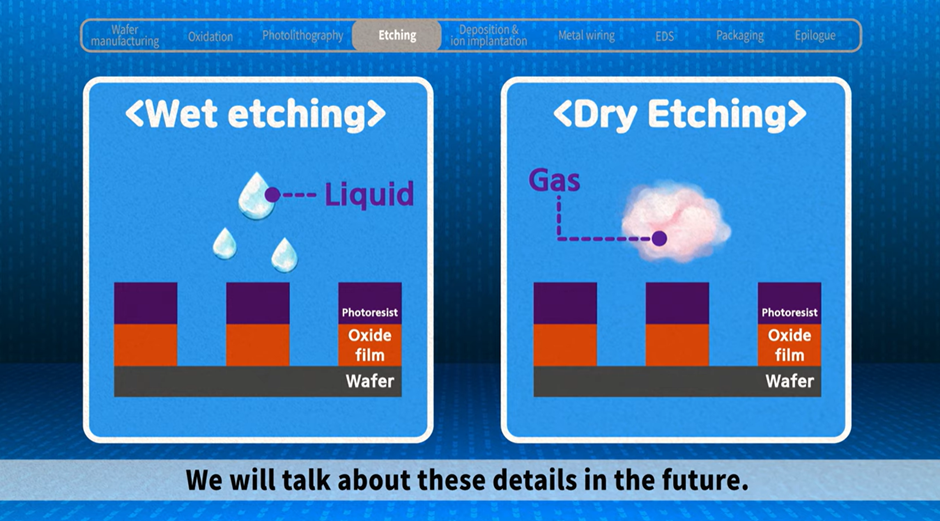
Next comes the etching process. Similar to the art form of ‘etching’, this step selectively carves out certain parts of the wafer. Materials in the areas without photoresist are removed by an etchant to leave behind only the desired circuit patterns on the wafer. The photoresist is removed once the etching process is complete. This process of creating desired circuit patterns is repeated on multiple layers.
There are different methods in etching, which are wet etching and dry etching depending on the materials used in the process. Dry etching uses reactive gases and ions to selectively remove unnecessary materials, whereas wet etching uses liquid chemical solutions.
Now that we have covered photolithography and etching, we understand how semiconductor circuit patterns are constructed. In the next installment, we will explore how these delicate layers are protected and how the circuits are finally connected.