[Editorial] Samsung’s Memory Innovation Opens Infinite Possibilities

Advancements in technology are the product of innovation, created by strong-willed, tenacious individuals who seize opportunities in a dynamic environment to achieve their goals.
The history of Samsung Memory has been a journey of persistent technological innovation, galvanizing our reputation as the leading memory solutions provider of the past three decades.
.
A Paradigm Shift to Unlock the Future of Memory
Memory’s main application evolved from PCs to mobile devices and now to data centers. Hyperscale AI is also rapidly gaining traction as memory’s newest application, and this will further expand to on-device AI, which operates natively on consumer devices like PCs and smartphones.
Of course, these trends also lead to evolving new needs for memory solutions.
To provide the best solutions for diversifying AI services provided by hyperscalers[1], we need high-performance, high-capacity and low-power memory products that can process a vast volume of data while also reducing Total Cost of Ownership (TCO). At the same time, differentiated memory products are also necessary to meet the needs of hyperscalers.
Furthermore, as data grows exponentially, the required role of memory is expanding from data storage — the intrinsic function of memory — to additional computational capabilities. Simply put, it is now time for memory solutions to share the data processing workload with the CPU and GPU.
.
Innovation for the Future, Beyond Limitations
In the memory business, securing cost competitiveness is crucial. This can be achieved by increasing density so wafers can yield more chips with higher capacity, and by realizing economies of scale using cutting-edge production facilities.
This is because previously, in the PC and mobile eras, demand for memory was heavily influenced by the product set’s Bill of Materials (BOM) cost. This dynamic is still in effect today, with BOM-centric structures generally determining demand.
The changing market environment has presented seemingly conflicting requirements, securing cost-competitiveness while supplying the highest-value-added products possible. In order to meet both, we have been carefully considering the path our memory business will take.
But the answer is simpler than you might think. Over the past 30 years, Samsung has led the industry by supplying customers with exactly what they need. And this principle is now more valid than ever. Although priorities vary, we strive to provide each and every aspect that our customers require in a product — including high-performance, high-capacity, low-power, custom and cost-competitive products.
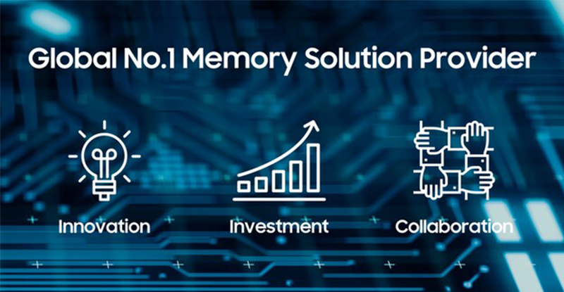
Of course, this is a challenging task. But Samsung aims to cement its position in the industry using three key strategies: First, to continually strive for innovations that overcome technological limitations. Second, to expand advanced process capacity and production of high-value-added products, while also increasing investment in R&D. Third, to build strong, symbiotic relationships with customers and partners.
.

.
As a fundamental part of its first key strategy, Samsung will increase the density of its DRAM and NAND flash to extreme levels and open new markets by offering differentiated solutions, including fully customized products for customers.
Unrivaled Technology Featuring the Highest Density
New structural and material innovations will be critical in the upcoming era of sub-10-nanometer (nm) DRAM and 1,000-layer vertical V-NAND. As such, we are developing 3D stacked structures and new materials for DRAM, while increasing layer count, decreasing height, and minimizing cell interference for V-NAND. We will continue to build on these strengths, which have enabled us to achieve the smallest cell size in the industry. Samsung is also working on the next generation of value-creating technologies, including a new structure that maximizes V-NAND’s input/output (I/O) speed.
Our 11nm-class DRAM is currently under development and on course to achieve the industry’s highest density. The ninth-generation V-NAND is well under way for mass production early next year with the industry’s highest layer count based on a double-stack structure.
Flagship Products Bringing Enhanced High-Performance, High-Capacity and Low Power
Samsung recently succeeded in developing the industry’s first 32Gb DDR5 DRAM. Moving forward, we will continue to expand the lineup of high-capacity DRAM, including 1TB modules. Furthermore, actively utilizing novel interfaces such as the CMM (CXL Memory Module) will help to realize a future in which memory bandwidth and capacity can be extended seamlessly, according to operational needs.
High Bandwidth Memory (HBM) is one of the most promising solutions for bringing enhanced value to customers in the AI era. In 2016, Samsung was the first company to commercialize HBM2 for HPC, laying the foundation for today’s HBM for AI market. We are currently mass-producing HBM3 while also making significant progress on the next-generation product, HBM3E. By fully utilizing proven technological capabilities garnered from years of mass- production experience — and based on partnerships with diverse customers — Samsung will provide high-performing HBM to customers and expand to customized HBM solutions.
LPDDR DRAM is a product specialized for low-power that achieves higher performance thanks to a new High-K Metal Gate[2] process. Samsung will expand its application to the PC market and data centers by using LPDDR5X CAMM[3]2 solutions, which are implemented in module form.
Expanding Memory Possibilities With Futuristic Solutions
To address memory bottlenecks, Processing-in-Memory (PIM) and Processing-near-Memory (PNM) — which enable data computation in the memory chip or at the module level — will be implemented into HBM and CMM products to dramatically improve data computation capabilities and increase power efficiency.
For server storage, we will soon introduce the Petabyte SSD (PBSSD), which can vary its capacity depending on application and supports petabyte-level scalability.
In line with its second key strategy, Samsung is focusing on increasing the proportion of high-value-added products and expanding advanced-process capacity, in response to the demand for new applications such as hyperscale AI. At the same time, we will continue to make investments and advance memory line operations to overcome demand volatility and long production lead times. Also crucial is investment for the future, exemplified by the building of a R&D line for cutting-edge semiconductors at our Giheung campus, which is the birthplace of Samsung’s memory business.
Following its third key strategy, Samsung will continue to build strong cooperative relationships with customers and partners. This includes the expansion of new product lines and markets through close collaboration on product planning, technology development and quality.
For example, through working closely with customers and partners of cloud services, devices, chipsets, and software — from the level of defining product specification — Samsung will expand the joint development of memory solutions optimized for next-generation systems and applications. This approach will serve to minimize data transfer latency and maximize bandwidth while dramatically increasing power efficiency. Simultaneously, we will strengthen cooperation with global partners, such as materials and equipment providers, to create a new generation of disruptive technologies.
.
Overcoming the Memory Challenges of Tomorrow
I believe that the accomplishments of Samsung have been made possible by the boldness of not fearing failure, the desire to achieve, and the drive to challenge the limits.
In the future, society will grow to be even more complex, and a more diverse range of new products and services will emerge as the IT industry develops. In response, Samsung will continue to grow together with our customers, creating a better future through continuous innovation and cutting-edge technology.
In the upcoming Samsung Memory Tech Day 2023 — which takes place in Silicon Valley, California, U.S. on October 20 — Samsung will introduce its latest memory technologies, products and future strategies. I hope you can join us to share in the bright future that will be enabled by Samsung Memory’s technologies.
.
[1] Hyperscalers: Corporations that run a large-scale data center.
[2] High-K Metal Gate: A technology that applies a new metal material to the gate level to minimize leakage currents.
[3] Compression Attached Memory Module (CAMM): LPDDR package-based module product.
.
Related tag
Related Stories
-
 2023.10.23Powering the Hyperscale AI Era: Next-Gen Memory Solutions Unveiled at Samsung Memory Tech Day 2023
 -
 2023.10.12Samsung System LSI Tech Day 2023: Experts Present Cutting-Edge Image Sensors and Automotive SoC
 -
 2023.10.12Samsung Austin Semiconductor Pumps $13.6 Billion into Central Texas Economy in 2022