Featured Stories
64 posts
-
Technology 2026.03.17
[Video] Architecting the AI Era: Samsung Electronics and NVIDIA Define the Future at GTC 2026
Samsung Electronics, a global leader in advanced semiconductor technology, took center stage at NVIDIA GTC 2026 to showcase its vision for the future of...
-
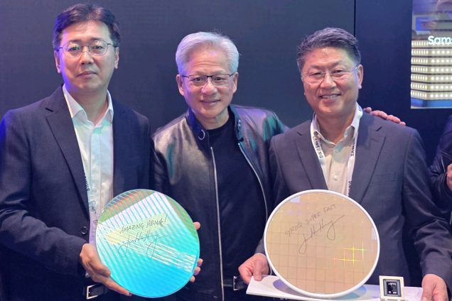
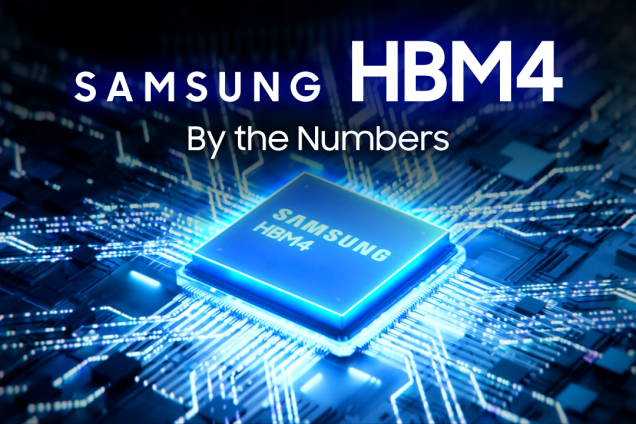
Technology 2026.03.13
[Video] The HBM4 Infographic: Key Specs and Performance Leap
Samsung Electronics has commenced mass production of HBM4 (6th-generation High Bandwidth Memory) and initiated commercial shipments to customers, marking...
-
Technology 2026.03.10
Samsung Launches Sokatoa to Enhance GPU Performance Analysis on Android
Bringing multi-frame GPU profiling, Sokatoa enables developers to identify and resolve complex graphics performance issues with greater speed and precision...

-
Technology 2026.01.09
[CES Innovation Awards® 2026 Honoree] Portable SSD T7 Resurrected: 100% Recycled Aluminum Body Case and Recyclable Packaging, Designed for Circular Resource Use
Samsung Semiconductor earned seven CES Innovation Awards® this year, demonstrating how semiconductor technology continues to drive innovation...

-
Technology 2026.01.09
[CES Innovation Awards® 2026 Honoree] Detachable AutoSSD: Industry’s First Detachable, High-Performance Automotive SSD
Samsung Semiconductor earned seven CES Innovation Awards® this year, demonstrating how semiconductor technology continues to drive innovation...

-
Technology 2026.01.09
[CES Innovation Awards® 2026 Honoree] PM9E1 M.2 22×42: High-Performance, Ultra-Compact PCIe Gen5 NVMe SSD Optimized for AI
This year, Samsung Semiconductor earned seven CES Innovation Awards®, demonstrating how semiconductor technology continues to drive innovation across...