About Samsung Semiconductor Newsroom
Samsung Semiconductor Newsroom is the official news platform for Samsung Electronics’ Device Solutions Division, providing the latest updates on the company’s semiconductor innovations and technologies, as well as industry trends.
Discover in-depth insights and cutting-edge advancements to stay informed with accurate and relevant information shaping the future of the semiconductor industry.
About Samsung Electronics’ Device Solutions Division
Samsung’s Device Solutions Division offers one of the most extensive product portfolios in the industry across three main businesses: Memory, System LSI and Foundry. Through bold business strategies, consistent investments and persistent commitment to innovation, we are one of the largest semiconductor companies in the world. We have been the leading memory provider in the industry for the past 30 years. Since 2002, building on our success in memory and we have widened our expertise into logic, providing leading logic chip solutions as well as foundry services. To deliver more optimized products and services to our customers, the Foundry Business later became an independent unit, separate from the System LSI Business.
It’s been an incredible journey, from humble beginnings to a global semiconductor powerhouse. The biggest challenges in technology have always driven us toward greater innovation, and even now, the endless possibilities of the future continue to excite us. We will remain relentless in exploring uncharted territories and pushing ourselves to be problem solvers. Our components will spark the imagination of device manufacturers and developers and continue to be the foundation for a better world.
Business Overview
Memory Business
Memory solutions have been driving the digital revolution, and for over three decades, Samsung’s Memory Business has been at the forefront of delivering milestone technologies that move the industry forward.
With leading performance, density and energy efficiency, Samsung’s DRAM and flash memory solutions have reshaped paradigms and are accelerating growth across the industry for applications from PC, mobile and gaming to next-generation data centers, enterprise servers and AI/ML.
Samsung’s DRAM technologies have been the optimum solution for the most demanding system requirements. The company continues to push boundaries by bringing new values to the market, such as the industry’s first application of extreme ultraviolet (EUV) technology, as well as added services for clients.
Since 2013, Samsung’s industry-first 3D V-NAND technology has also overcome the challenges posed for previous data storage devices while offering unprecedented scalability that will continue to address the ever-increasing needs for data processing and storage systems.
System LSI Business
As our lifestyles become more connected and on-the-go, so do our devices, enabling added freedom and intelligence in our digital experiences. Samsung’s System LSI Business designs powerful yet energy-efficient logic semiconductors, such as mobile processors, image sensors and display driver ICs (DDI) for various applications including mobile, automotive and IoT.
The Exynos family, Samsung’s lineup of mobile processors, are the brains of devices across the IT landscape. Available in the industry’s most advanced process technologies, as well as with multi-mode modem and connectivity solutions, Samsung’s mobile processors bring outstanding performance and efficiency to meet the demands of today’s smart devices.
Samsung’s ISOCELL image sensors allow us to capture DSLR-level images with vivid color and brightness, even in challenging lighting environments. While reducing pixel sizes for the latest mobile devices, Samsung’s advanced pixel technologies offer comprehensive solutions that enhance the overall mobile imaging experience.
Samsung is also a leading provider of a variety of cutting-edge LSI solutions, including security ICs, DDIs, smart card ICs and PMICs, which are essential components in our digital devices.
Foundry Business
Samsung initiated its foundry business in 2005 and established it as an independent business unit in 2017 to better serve its customers. As a pure-play foundry provider, Samsung’s Foundry Business brings state-of-the-art process technologies, ranging from EUV-based 5nm to 3nm GAA, 28nm FD-SOI to 14/10/8/5/4nm FinFET, as well as 8-inch and specialty processes. These capabilities enable a multitude of new opportunities for emerging applications such as high-performance computing (HPC), AI, 5G, mobile and automotive.
By leveraging Samsung’s longstanding chip fabrication expertise along with its Samsung Advanced Foundry Ecosystem (SAFE™) program, Samsung’s Foundry Business is a trusted partner that supports global fabless and IDM semiconductor customers for their market success.
Samsung offers a full range of verified EDA/DM solutions, product-proven intellectual property (IP) and a flexible design environment through cloud-based tools, comprehensive ASIC design, as well as packaging and testing services.
History
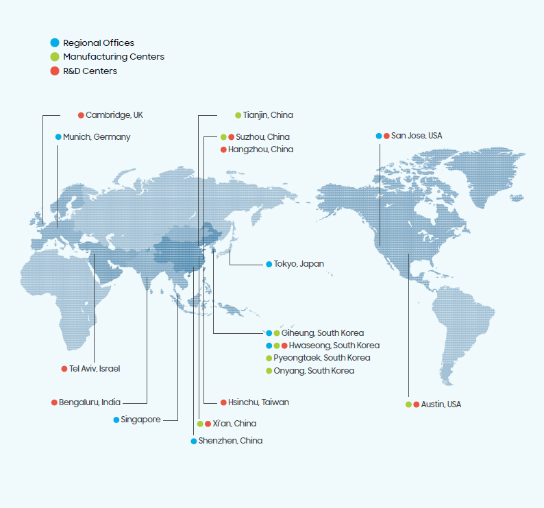
Global Network