Memory Innovation Powering a New AI Infrastructure Cycle Part 2


Samsung Memory Solutions Connecting the Future of Edge AI
In Part 1, we explored how the expansion of edge AI is making capacity, bandwidth, and energy efficiency critical challenges for AI systems. As the industry works to address these challenges, the role of memory is also being redefined.
Memory: A Key Technology for Overcoming AI System Bottlenecks
In the past, memory primarily served to store and deliver data required for computation. In the AI era, however, it is evolving into a core technology that determines overall system performance and energy efficiency.
For edge AI in particular, memory must deliver high capacity, high bandwidth, and low power consumption simultaneously. It must store more data within a limited space, deliver that data quickly enough to prevent xPUs from remaining idle, and reduce the energy consumed in moving data.
The parallel growth of cloud and edge AI is also creating new opportunities for the memory market. In the cloud, large-scale model training and high-performance inference are increasing demand for server-grade, high-bandwidth and high-capacity memory. At the edge, real-time inference and personalized data processing are generating demand for memory solutions optimized for new device form factors and power conditions.
Data generated and accumulated at the edge can be used to further enhance models in the cloud, while models developed in the cloud can be optimized and deployed back to edge environments. Within this virtuous cycle, edge AI does not replace the existing cloud memory market. Instead, it expands the scope of AI applications and becomes a new growth engine for the overall memory semiconductor market.
Samsung Memory Solutions Overcoming Bottlenecks Through Next-Generation 3D Architectures
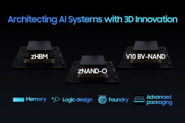
Samsung Electronics is introducing a range of next-generation memory solutions to overcome the capacity, bandwidth, and power-efficiency limitations facing edge AI. These include zHBM, based on a 3D memory architecture that shortens the physical distance between processors and memory; zNAND-O, a 3D NAND solution optimized for edge AI; and LPDDR-PIM, which integrates computing capabilities directly into memory.
Together, these solutions can alleviate data-movement bottlenecks while improving system-wide performance and energy efficiency.
zHBM: A Next-Generation Architecture That Shortens Data-Movement Distances
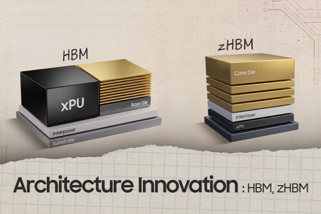
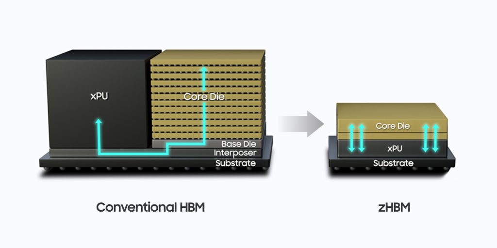
Conventional HBM uses a 2.5D architecture in which HBM and an xPU are positioned side by side on a silicon interposer. Through high-density interconnections enabled by the silicon interposer and the vertical stacking of memory dies, HBM has already reduced data-movement distances significantly compared to conventional 2D structures. However, the physical distance that still remains between the memory and the processor continues to limit further improvements in bandwidth and energy efficiency.
zHBM is a next-generation 3D memory architecture that overcomes these limitations by directly integrating the xPU and HBM in a vertically stacked configuration. By combining wafer-on-wafer integration with HCB, or hybrid copper bonding, zHBM enables direct copper-to-copper connections, achieving much higher vertical interconnect density and greater parallelism than conventional HBM. It is also designed to achieve higher bandwidth and energy efficiency without excessively increasing the data rate per pin by adopting a distributed I/O architecture that distributes data paths across multiple I/O channels.
Shortening the data path between the processor and memory makes it possible to transfer more data at higher speeds while significantly reducing the energy required for data movement. It can also reduce reliance on complex high-speed interface circuitry and enable greater integration density and bandwidth within a limited system footprint.
This structure, however, triggers an important thermal-management challenge because heat generated by the xPU must pass through the memory stack. zHBM aims to reduce thermal resistance and secure a more efficient thermal path by optimizing stack height and structure and applying HCB.
Through these architectural innovations, zHBM opens up new possibilities for significantly increasing performance per system and performance per watt while reducing thermal resistance beyond the incremental improvements achieved from one HBM generation to the next. This represents more than a simple increase in bandwidth. It is a fundamental transformation of how memory and processors are positioned and interconnected.
Each xPU has unique requirements in terms of performance, power, thermal characteristics, and physical dimensions. For this reason, zHBM cannot be fully optimized as a standalone memory product. The xPU and zHBM must be jointly developed and optimized from the earliest stages of design, making precise co-optimization of logic and memory increasingly important.
This architecture has the potential to extend the limits of bandwidth and energy efficiency not only in large-scale cloud AI systems, but also, over the longer term, in high-performance edge AI systems with significant space and power constraints.
LPDDR-PIM: Computing Within Memory
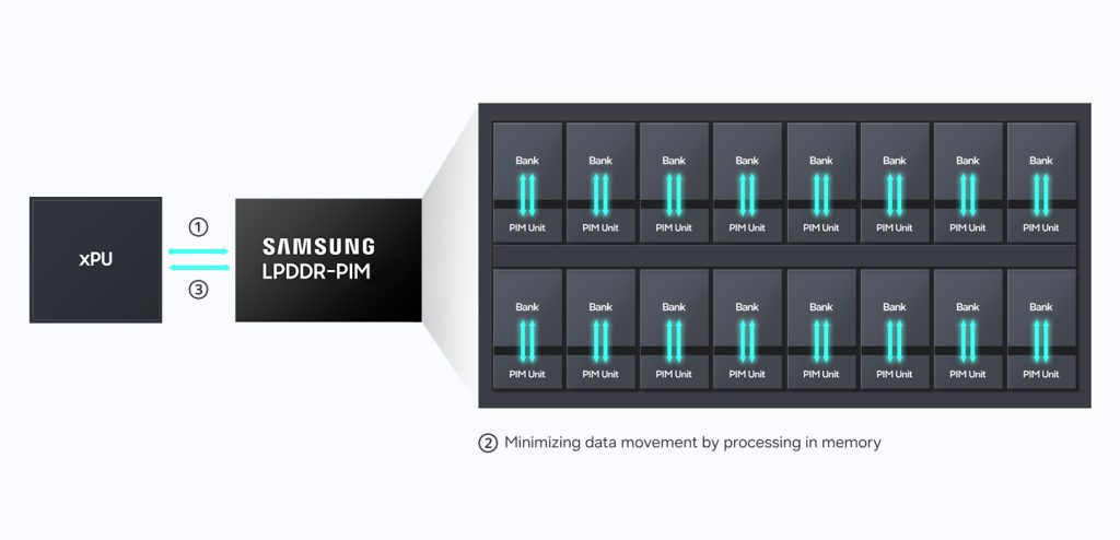
PIM, or processing-in-memory, reduces data movement by integrating computing capabilities directly into memory. LPDDR-PIM applies PIM technology to low-power LPDDR, enabling selected computations to be performed within memory instead of repeatedly transferring data to an xPU.
This approach can reduce the bottlenecks and power consumption associated with data movement while improving AI inference performance and energy efficiency. It offers significant potential for AI workloads that involve repetitive data processing and for edge AI environments that require high performance within a limited power budget.
zNAND-O: Rapidly Supplying Large-Scale AI Data
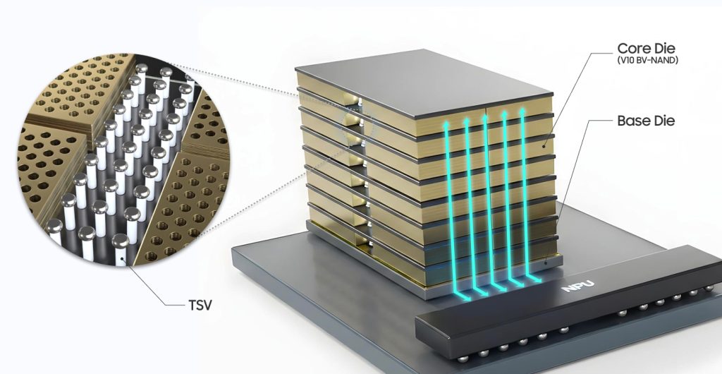
zNAND-O is a next-generation memory solution that combines high-performance, high-capacity NAND with 3D packaging technology to create a new data tier between DRAM and conventional NAND storage. By vertically integrating multiple NAND dies, zNAND-O is designed to increase capacity and I/O performance within a limited footprint while delivering faster data access and greater power efficiency than conventional NAND.
zNAND-O provides higher bit density than DRAM while significantly improving read performance and power efficiency compared with conventional NAND flash. It also targets microsecond-level latency and high bandwidth, supporting high-performance data processing with low power consumption. This enables greater scalability and flexibility even within space-constrained systems.
Samsung is proposing a new NPU-centric memory architecture that uses zNAND-O to optimize data placement within AI systems. In this architecture, the operating system and KV cache are placed in DRAM, while large, read-intensive model weights are stored in zNAND-O. This reduces dependence on DRAM and can address both memory cost and capacity challenges while minimizing performance degradation.
zNAND-O also demonstrates the potential to significantly improve memory architecture efficiency while maintaining performance comparable to conventional UMA-based DRAM systems. This is expected to provide a foundation for reliably running larger AI models in on-device environments.
For edge AI environments such as AI workstations and AI PCs, where real-time processing of large-scale data is essential, zNAND-O can evolve into a new memory tier that complements the capacity and cost limitations of DRAM and the performance limitations of conventional NAND storage.
Samsung’s Integrated Capabilities Connecting Cloud and Edge AI
AI is not simply moving from the cloud to the edge. Large-scale cloud computing and real-time, personalized edge AI are expanding each other’s roles and creating a new infrastructure ecosystem.
In this process, memory is becoming more than a component that stores data. It is emerging as a core technology that determines the actual performance and energy efficiency of AI systems. As AI expands across more devices and industries, technologies that deliver greater capacity and bandwidth within limited space and power budgets will become increasingly important.
Optimizing an entire AI system requires more than improving the performance of individual semiconductor chips. Memory, logic, interfaces, and packaging must be considered together from the earliest stages of product design to address the complex trade-offs among capacity, bandwidth, power efficiency, thermal characteristics, and form factor.
Samsung has broad capabilities across memory, logic, foundry, and advanced packaging. Based on these integrated capabilities, Samsung is advancing DTCO, or Design-Technology Co-Optimization, to jointly optimize design and process technologies and connect memory, logic, and packaging from a system-level perspective.
Next-generation memory based on 3D integration, in particular, cannot be realized through standalone DRAM or NAND technologies alone. A wide range of technical elements must be designed and integrated organically, from high-performance logic dies and advanced process technologies to die-to-die interconnects, power delivery, thermal management, and advanced packaging.
Samsung’s end-to-end semiconductor capabilities provide a differentiated foundation for addressing these complex challenges in an integrated manner and improving not only the performance and power efficiency of next-generation products, but also the overall completeness of the system.
Samsung will continue to innovate beyond the traditional boundaries of memory, logic, and packaging, enhancing the performance and efficiency of AI infrastructure from the cloud to the edge and further strengthening its technology leadership for the new AI era.