A Scale Beyond Imagination: Inside Samsung’s Massive Semiconductor Fabs


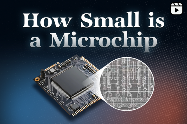
The tiny semiconductor chips embedded in our daily devices—from smartphones and laptops to cars—are marvels of modern technology. But the journey of these microscopic components begins in a space of almost unimaginable proportions. We invite you to explore the sheer scale of a Samsung semiconductor fabrication plant (FAB), the heart of our technological leadership and the starting point of our strategy for clear innovation-driven differentiation.
Putting Scale into Perspective: Beyond World Landmarks
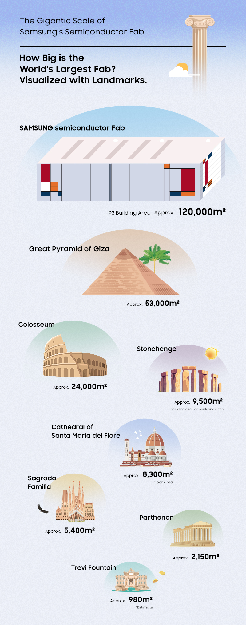
It’s difficult to truly comprehend the size of a semiconductor fab. To help, we can compare its footprint to some of the most famous landmarks in the world.
Even colossal ancient structures like Rome’s Colosseum (approx. 24,000 m²) or Egypt’s Great Pyramid of Giza (approx. 53,000 m²) are dwarfed by a single Samsung fab. The building area of just one of our fab facilities measures approximately 120,000 m²—more than twice the size of the Great Pyramid and five times larger than the Colosseum. It also far exceeds the expanse of world-famous public squares like the Place de la Concorde in Paris (approx. 86,400 m²).
The Numbers Behind the Scale: The Pyeongtaek Campus
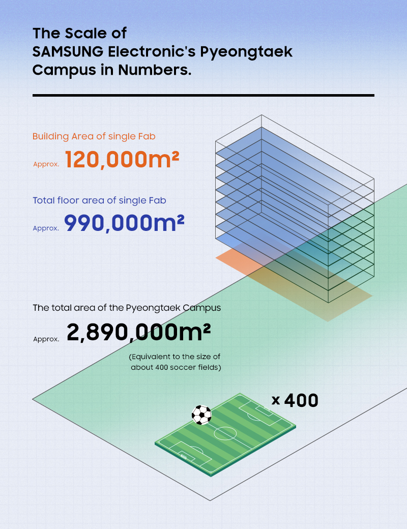
Not just in visuals, the numbers speak for themselves. The scale of our Pyeongtaek campus, a hub of semiconductor manufacturing, is staggering:
- Building Area (single fab): approx. 120,000 m²
- Total Floor Area (single fab): approx. 990,000 m²
- Total Pyeongtaek Campus Site: approx. 2,890,000 m² (400 soccer fields)
This footprint houses the vast, ultra-clean environments known as cleanrooms and cutting-edge equipment that drive hundreds of complex, precise manufacturing processes around the clock.
Where Great Innovation Begins
This immense scale is more than just a matter of size; it represents a relentless investment in the future of technology. It is the foundation upon which we build the next generation of semiconductors that will power future advancements.
This is where innovation takes root. Today, that process begins right here, at the core of Samsung’s semiconductor operations: the fab.